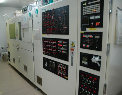
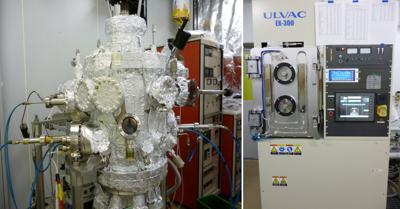
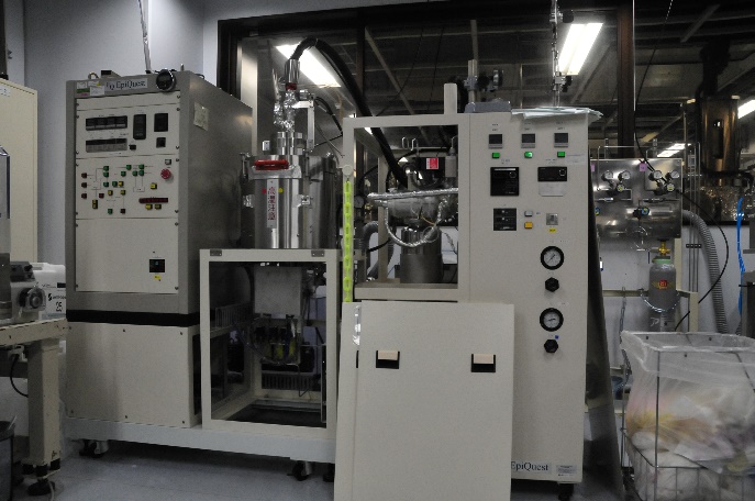
Organo-Metallic Vapor-Phase-Epitaxy (OMVPE) system for the growth of GaInAsP and AlGaInAs for use in optical devices. We have TMGa, TEGa, TMAl, TMIn, ZnH6, AsH3, PH3 and CBr4 for precursors.
This equipment draws arbitrary patterns by electron beam numerical control. The spot size of 5nm can be achieved. We have two systems which have the acceleration voltages of 50 and 100 keV.
This equipment is used for fabrication of DFB lasers and Silicon photonics circuits.
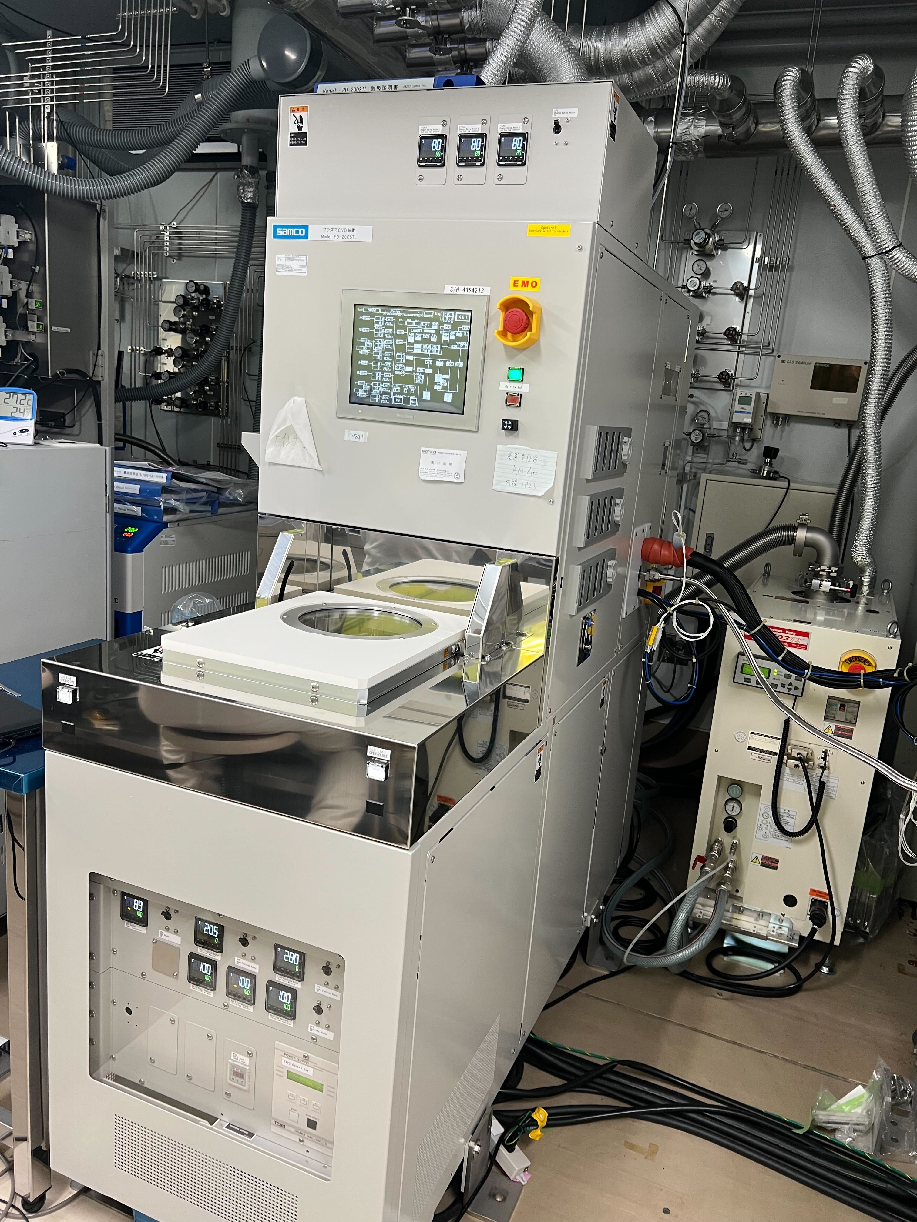
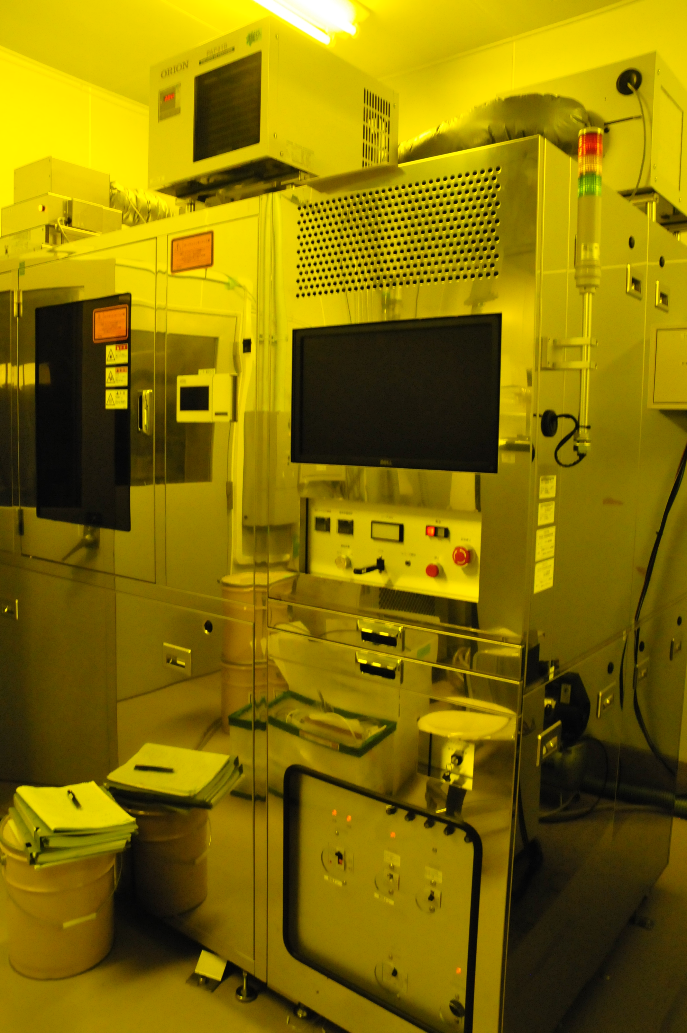
This equipment is plasma CVD (Chemical Vapor Deposition) system. Plasma CVD is a technique for depositing a thin film on the wafer by plasma assisting. This equipment is used for SiO2 layer deposition and the precursor is TEOS. We have two types of equipment, which have anode and cathode type electrode.
This equipment is plasma CVD (Chemical Vapor Deposition) system. Plasma CVD is a technique for depositing a thin film on the wafer by plasma assisting. This equipment is used for a-Si or SiN layer deposition and the precursor is TEOS.
CVD (Chemical Vapor Deposition) is a means of forming high-purity films on heated substrate surfaces by decomposing compounds containing raw material elements with plasma to induce chemical reactions. In our laboratory, trisilylamine is used as a raw material gas, N2O flows through it, and plasma is generated to form SiON films on the substrate.
RIE: Reactive Ion Etching
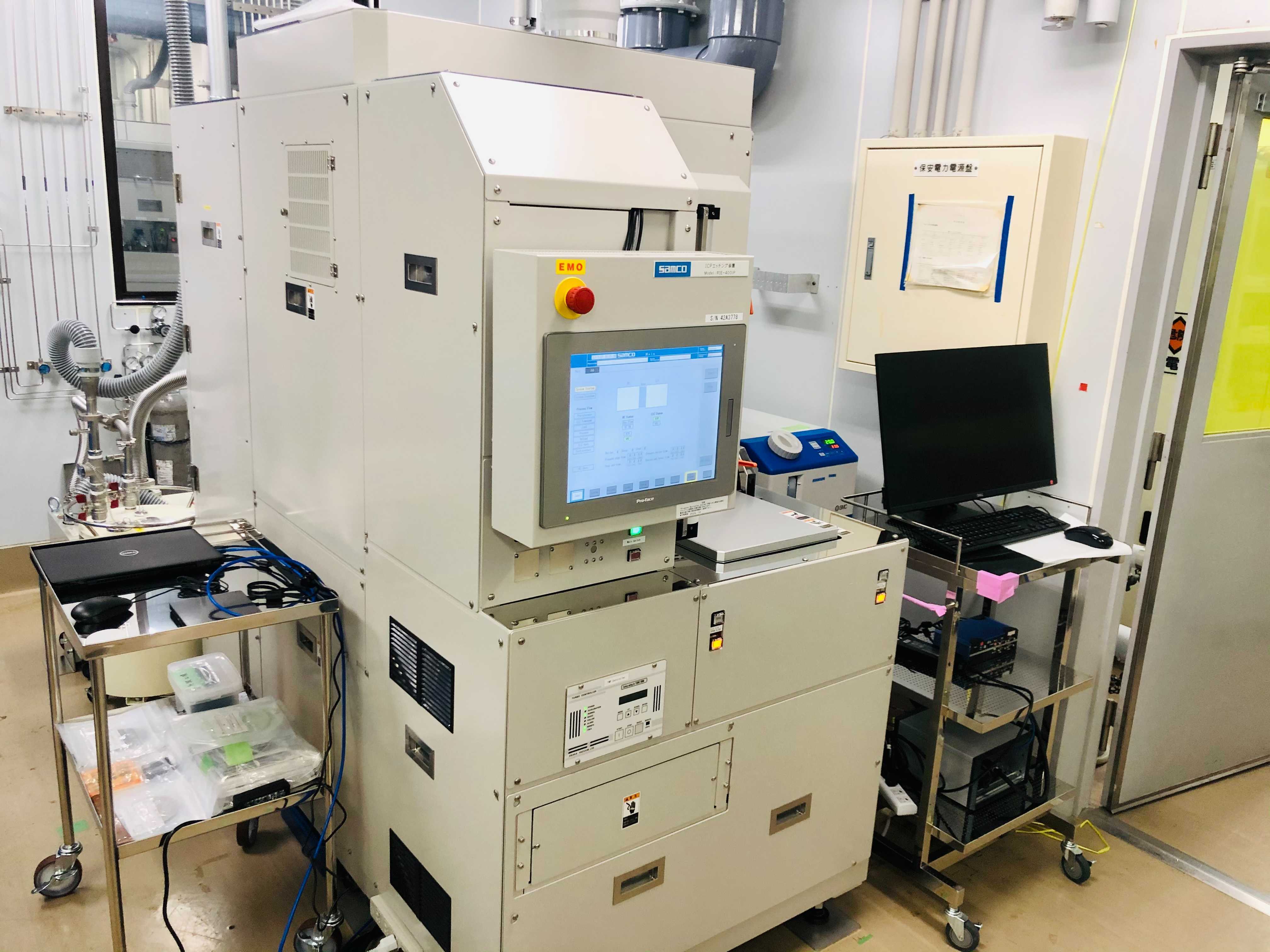
Fully automatic reactive ion etching system. The controllability and reproducibility of the pattern shape and the pattern etching dimension system are high, enabling low-damage processing with CH4 and CF4 for III-V materials and SiO2, respectively, can be done.
High-density ions are generated by the inductively-coupled plasma method, enabling high-speed anisotropic etching of various semiconductor materials. This system is used for Si etching in Si photonics.
compared with the system #1, stability of plasma is improved at low pressure. This system is mainly for Diamond etching as well as some topological structure.
Equipment for depositing metal.
Energy is given to the metal sources using the Electron-gun to form a metal thin film.
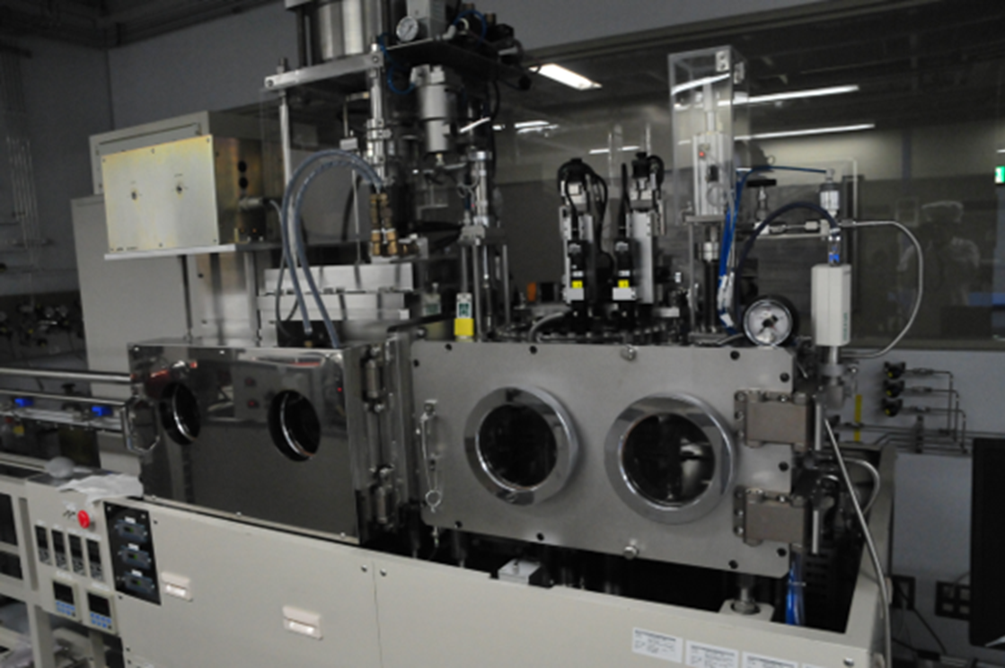
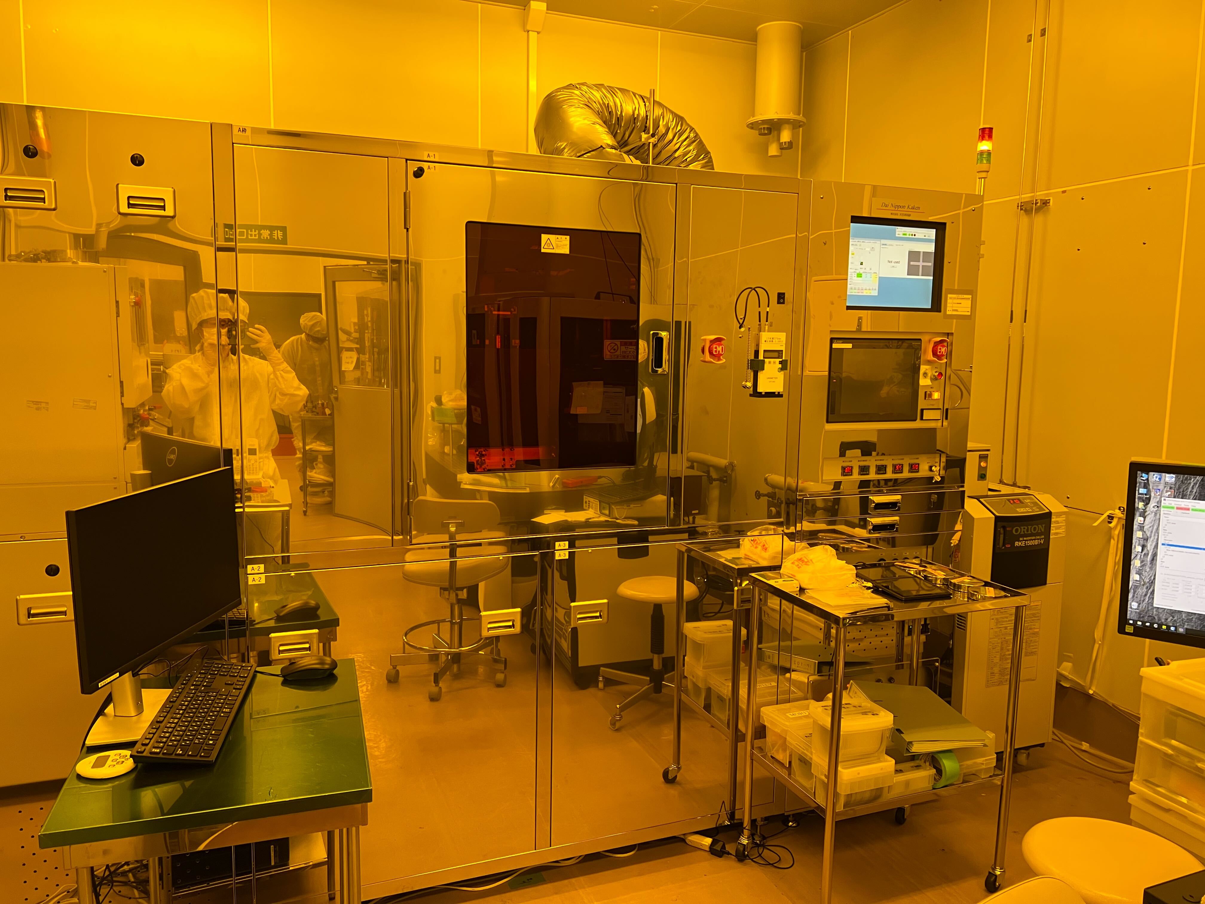
This device joins two different dissimilar material wafers.
Our laboratory mainly uses it for bonding III-V compound semiconductor wafers and Si wafers.
Activates the wafer surface by plasma in a vacuum chamber.
This device joins two different dissimilar material wafers.
Our laboratory mainly uses it for bonding III-V compound semiconductor wafers and Si wafers.
Activates the wafer surface by fast atom beam in a vacuum chamber.
This is direct transfer bonding (DTB) system which enables chip-on-wafer bonding even the wafer size are different. We do not need Pick and Place equipment and can directly bond the chips after dicing to any place we want. They system support up to 200 mm wafers.
This is a device for cleaning wafers using a special brush or ultrasonic waves.
Used for pretreatment of wafer bonding.
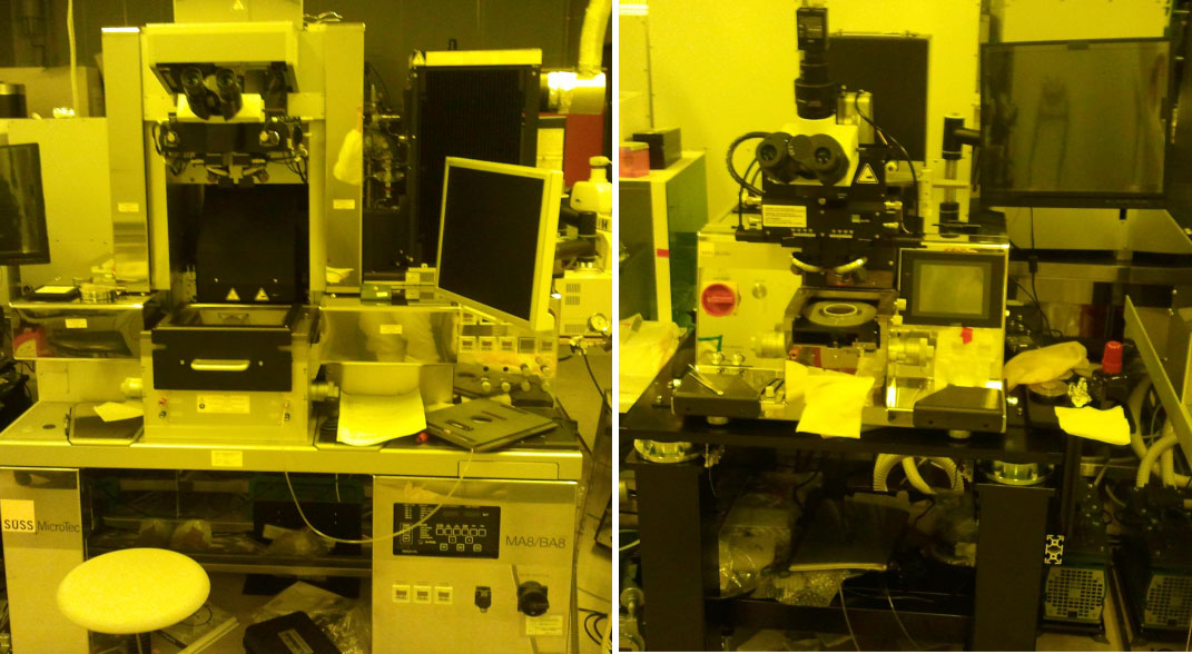
Equipment used for photolithography.
The mask pattern is transferred to the resist formed on the wafer surface.
Equipment used for photolithography.
Unlike a mask aligner, a pattern is drawn directly on the resist using DMD mirror and UV laser.
Equipment used in photolithography.
It has better resolution than the above.
This is a device for cleaning the mask used in the mask aligner.
Although this system was originally designed for imprinting resist, we are using this for polymer bonding in membrane laser process.
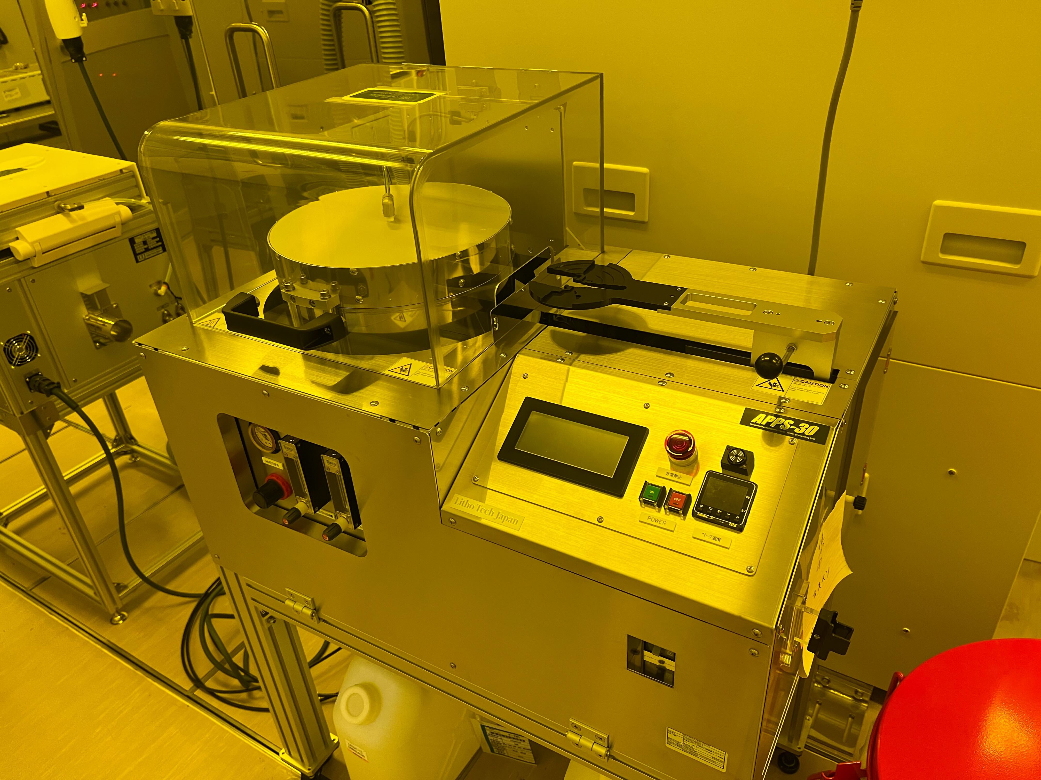
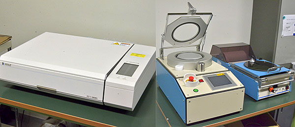
Equipment used for resist film formation.
This equipment is used for resist deposition and development. It is used for high precision uniformity, improved resist application and development options, and stable conditioning operation.
Manual HMDS bake process equipment that reacts at high temperature by pouring vaporized HMDS (hexamethyldisilazane). After wafers are manually set, HMDS baking is performed automatically.
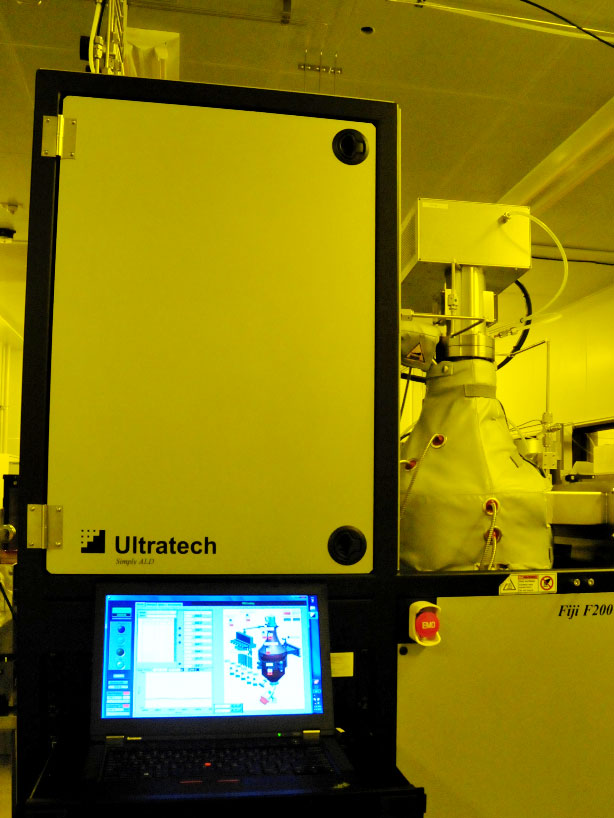
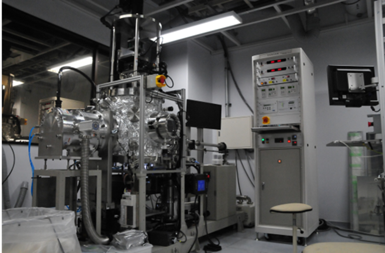
This device can form atomic layers one by one on the wafer surface.
By repeating, you can increase the number of layers. This system is used for mesa-side coating for laser process.
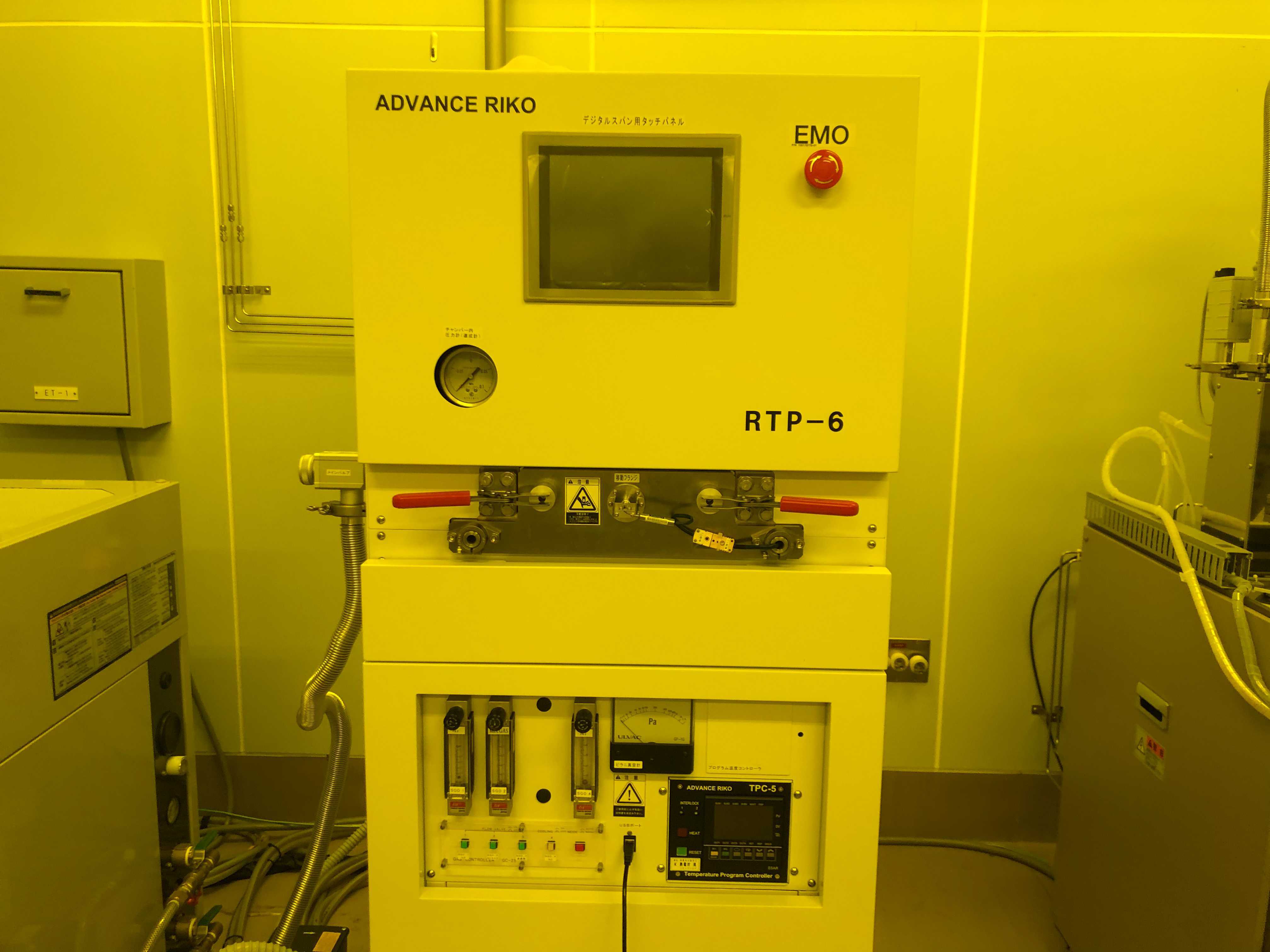
This system can rapidly heat a wafer to a high temperature.
The system is used for annealing contact metal to reduce the resistance.
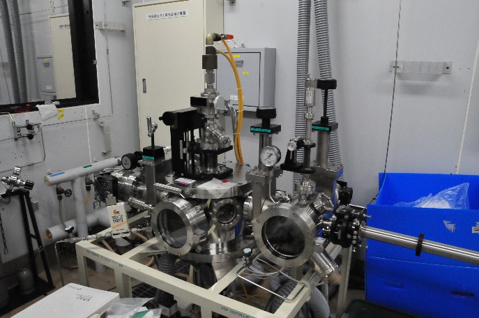
This is a device for forming dielectrics for high-reflection and anti-reflection coatings.
The accelerated ions are applied to the target, and the material flying from the target adheres to the wafer, forming a film.
This system can flatten the surface of the wafer with a chemical polishing agent and polishing pad. We use this for making 3D photonic circuit and wafer bonding.
A system that can perform steam oxidation to oxidize AlAs and AlInAs for VCSEL and in-plane laser current confinement purpose.
This system is mainly used for making chip of Si photonics.
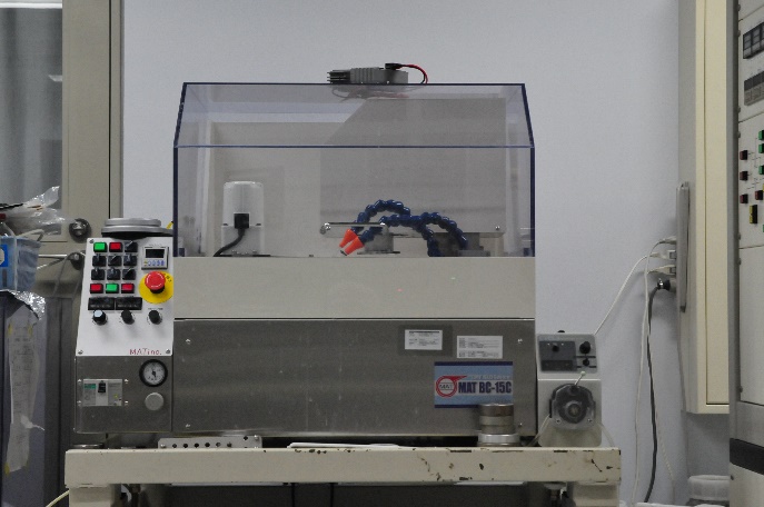
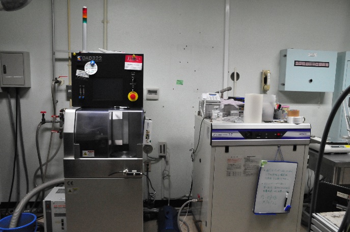
High-strength wafers can be cut using a high-speed rotating blade.
This is a group of devices for accurately dividing semiconductor wafers and small pieces.
A group of equipment that makes it easy to take out a divided wafer without damaging the end surface and breaking it.
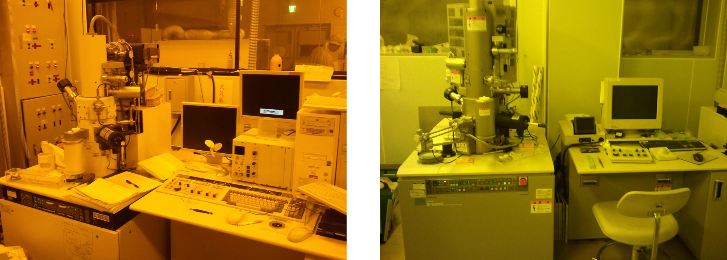
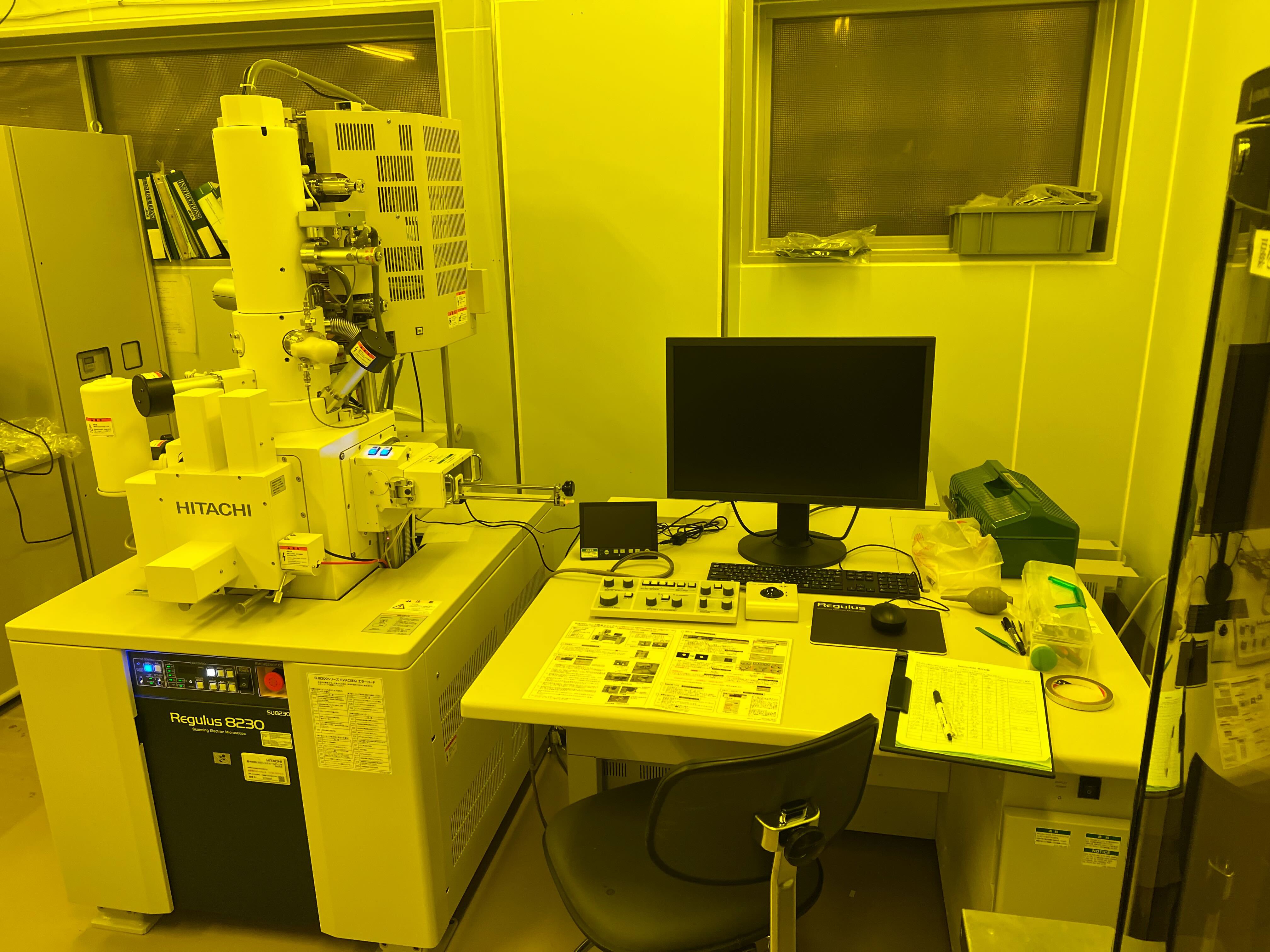
A device that hits an object with an electron gun, detects its secondary electrons, and projects it as an image.
Used when observing fine structures on the order of nanometers.
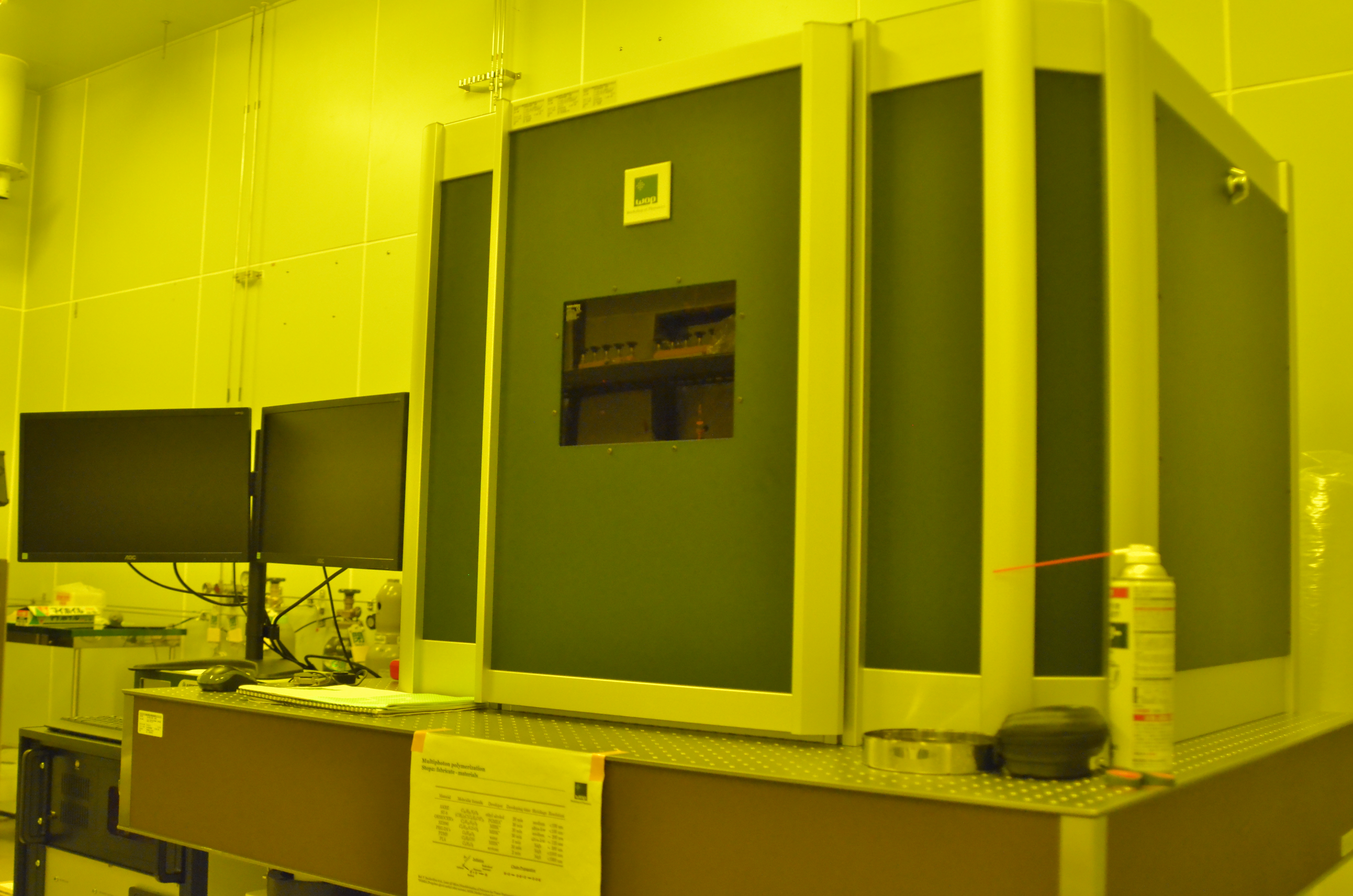
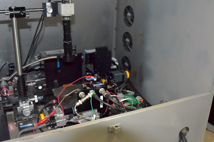
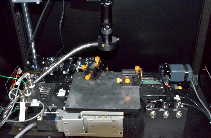
By irradiating a femtosecond laser, you can create an arbitrary three-dimensional pattern by computer control. Resolution <200 nm.
A device that hits an object with an electron gun, detects its secondary electrons, and projects it as an image.
Used when observing fine structures on the order of nanometers.
The new Cold Field Emission (CFE) gun is optimized for high-resolution imaging at low acceleration voltages. This CFE gun can magnify high-resolution images up to 2 million times.
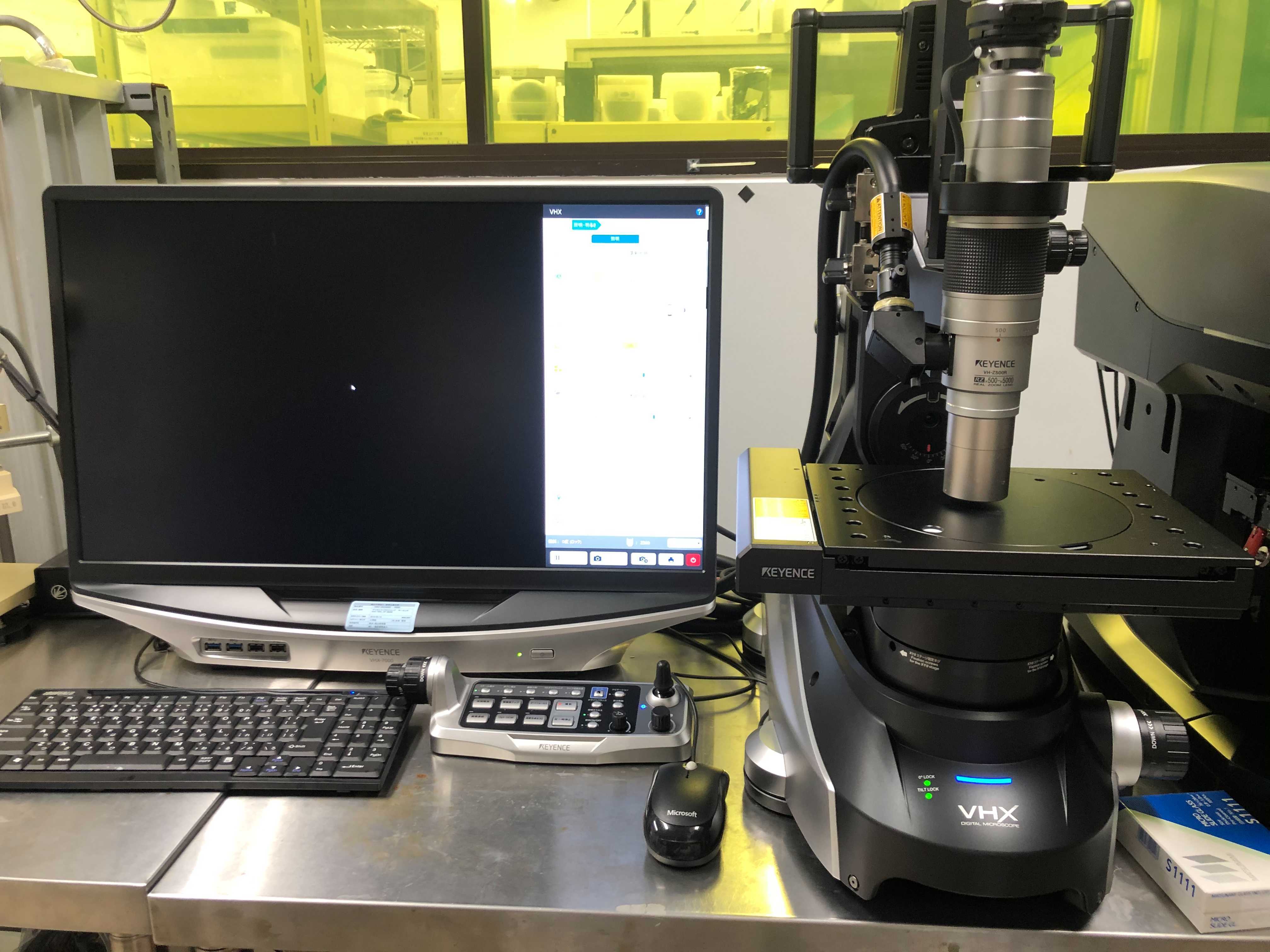
Visualize surfaces in 3D with real-time depth composition.
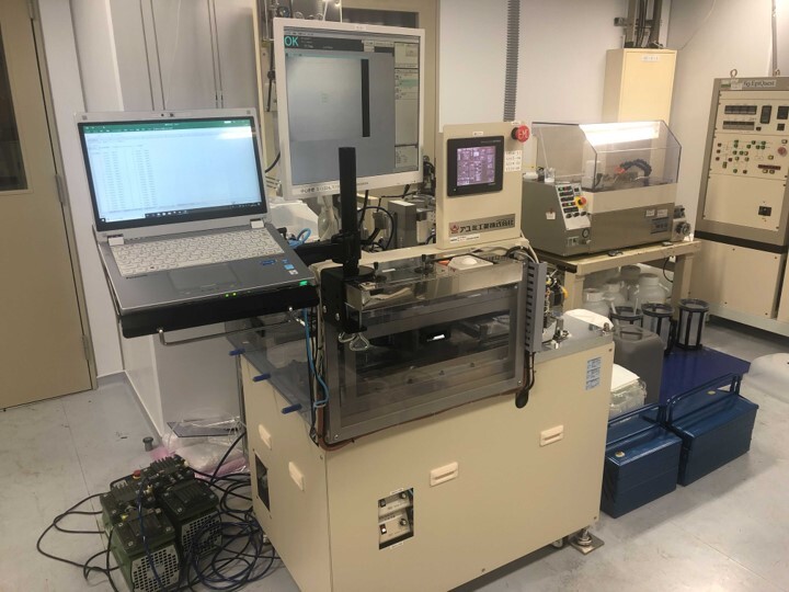
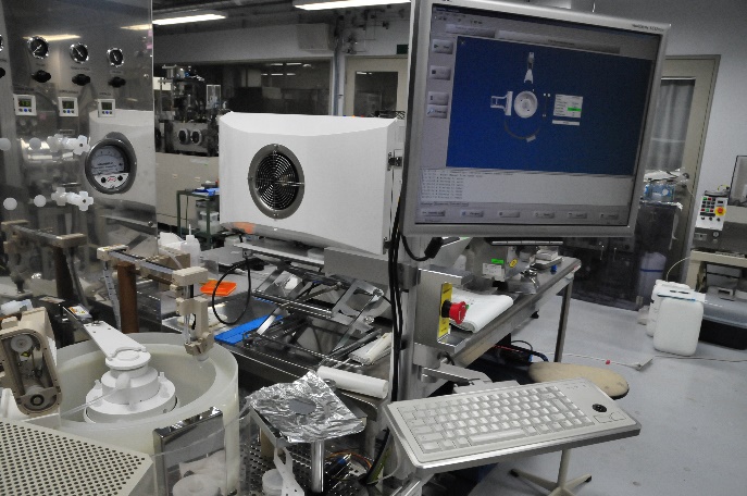
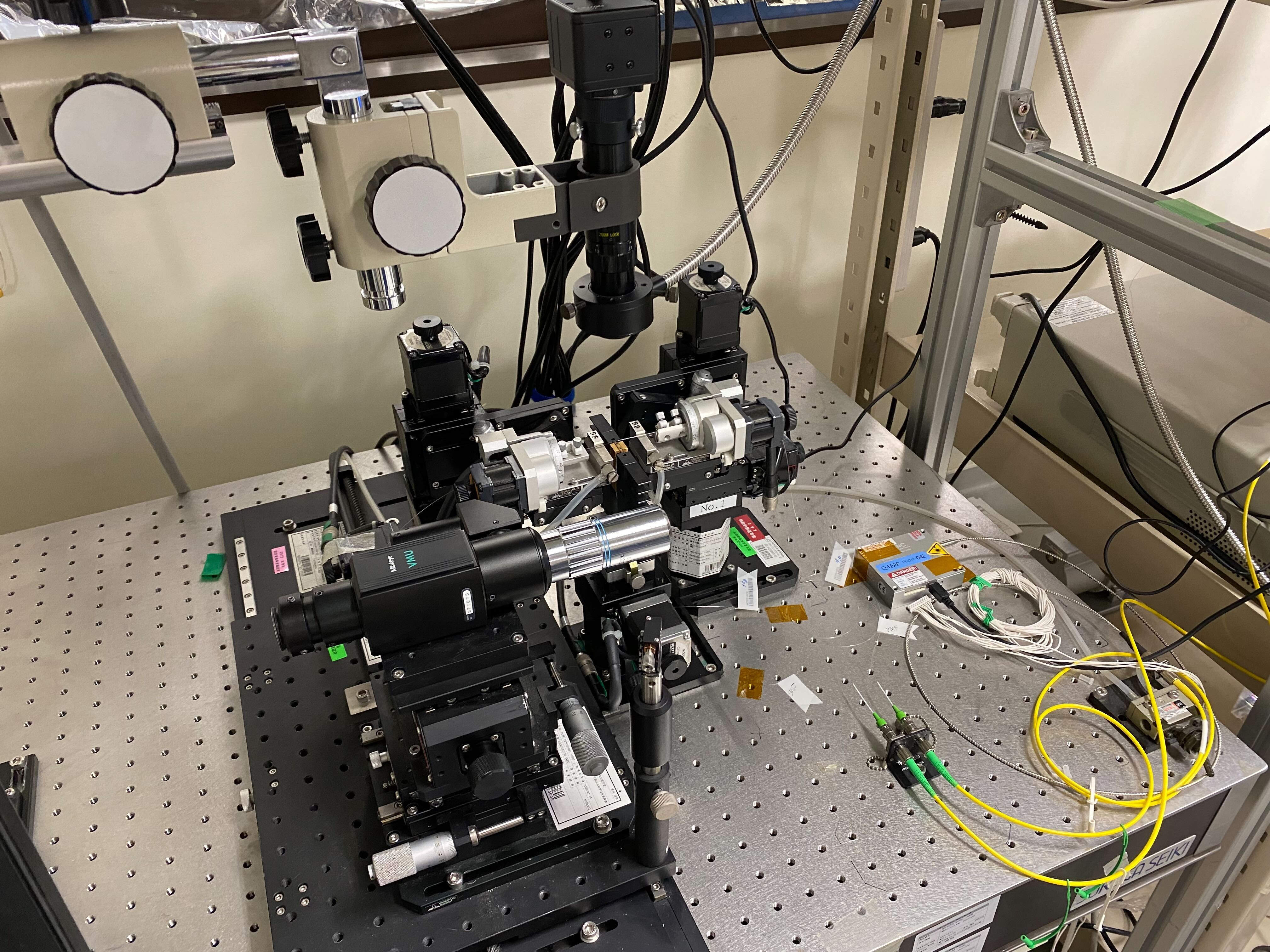
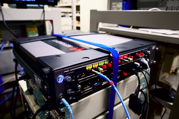
This device can automatically measure multiple bar-shaped elements. It can automatically measure not only current-light and current-voltage characteristics but also laser characteristics such as temperature characteristics, spectra, far-field images, near-field images, and polarization.
This device can measure the lifetime of laser.
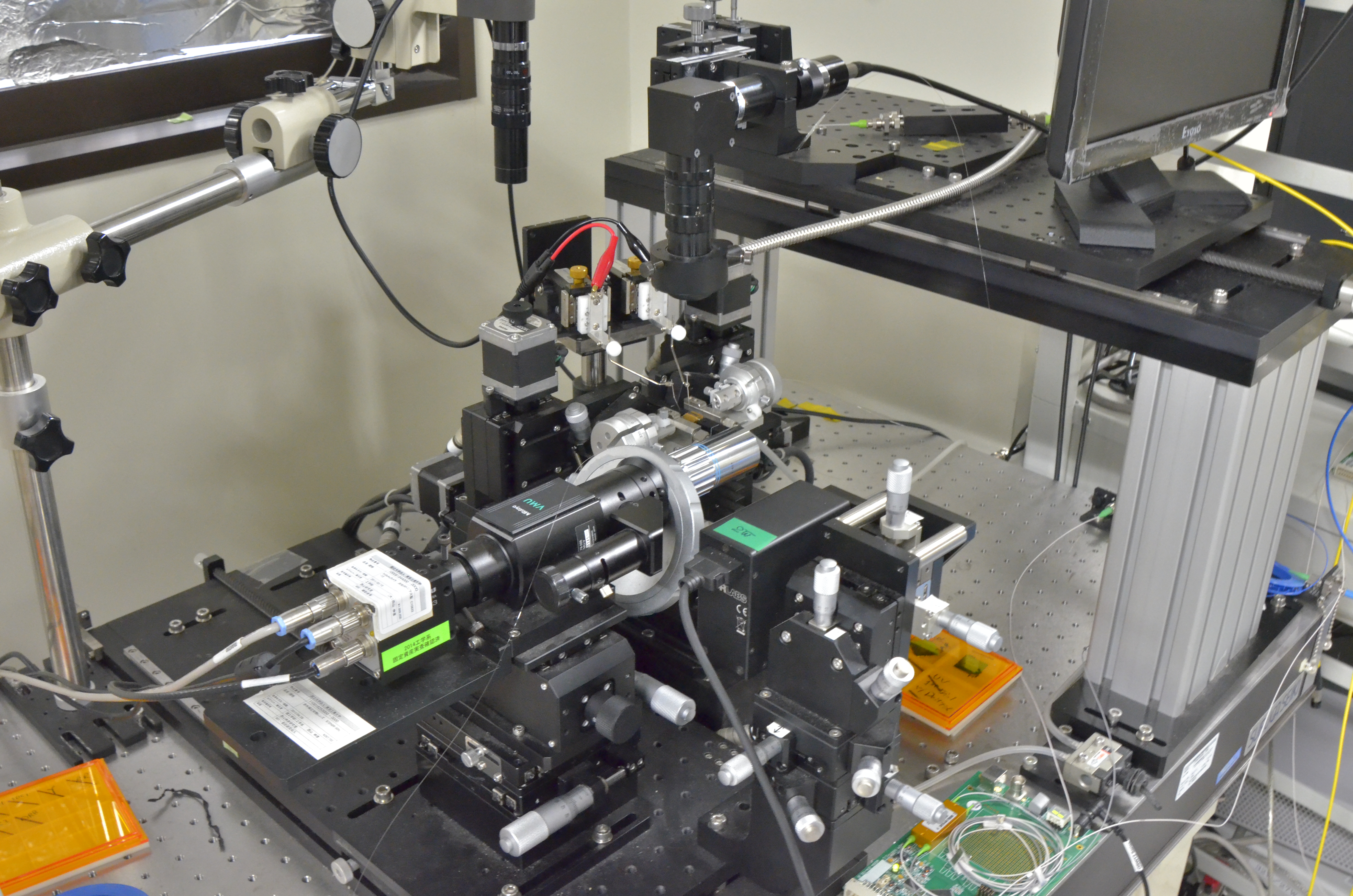
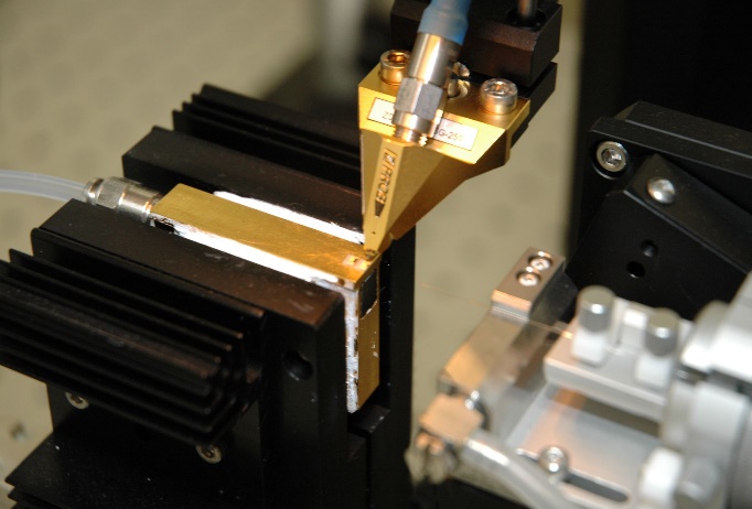
A device that can measure the transmission characteristics of multiple bar-shaped elements.
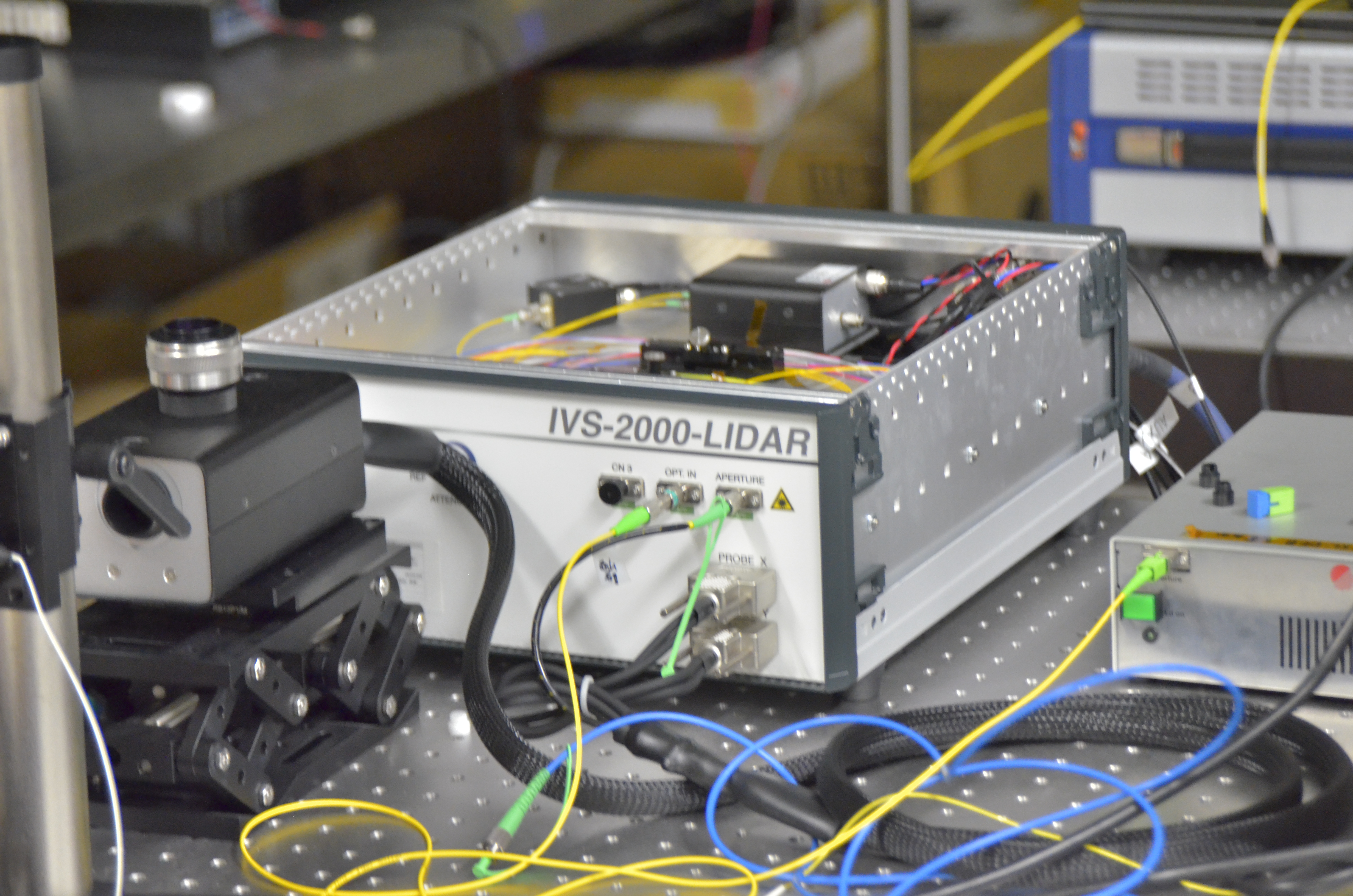
This device can measure coherent FMCW LiDAR.
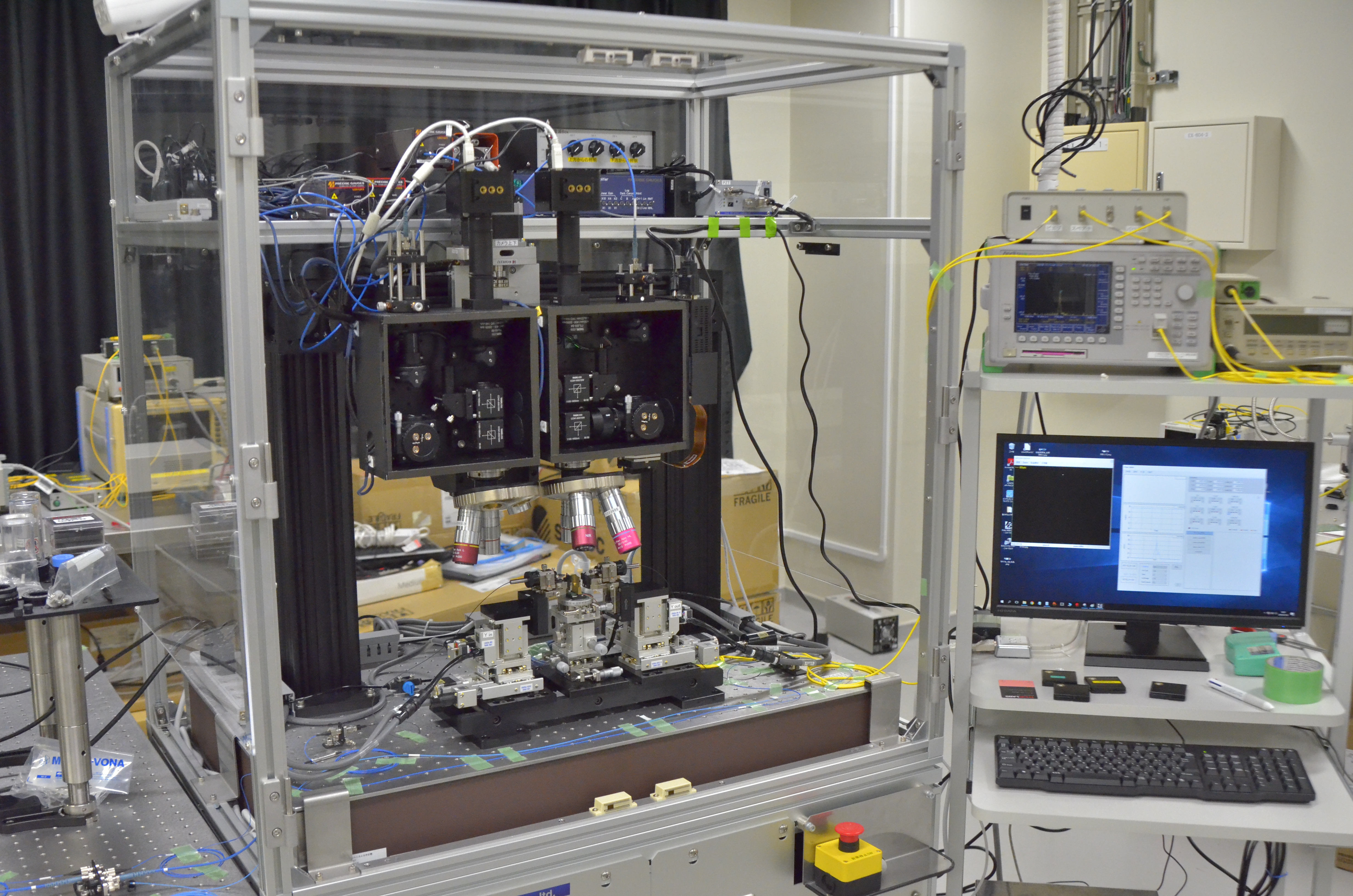
A device that can measure the transmission characteristics of multiple bar-shaped elements. In addition to fully automatic alignment, spatial phase modulated 1550 nm light and 980 nm light can be incident on the element from above.
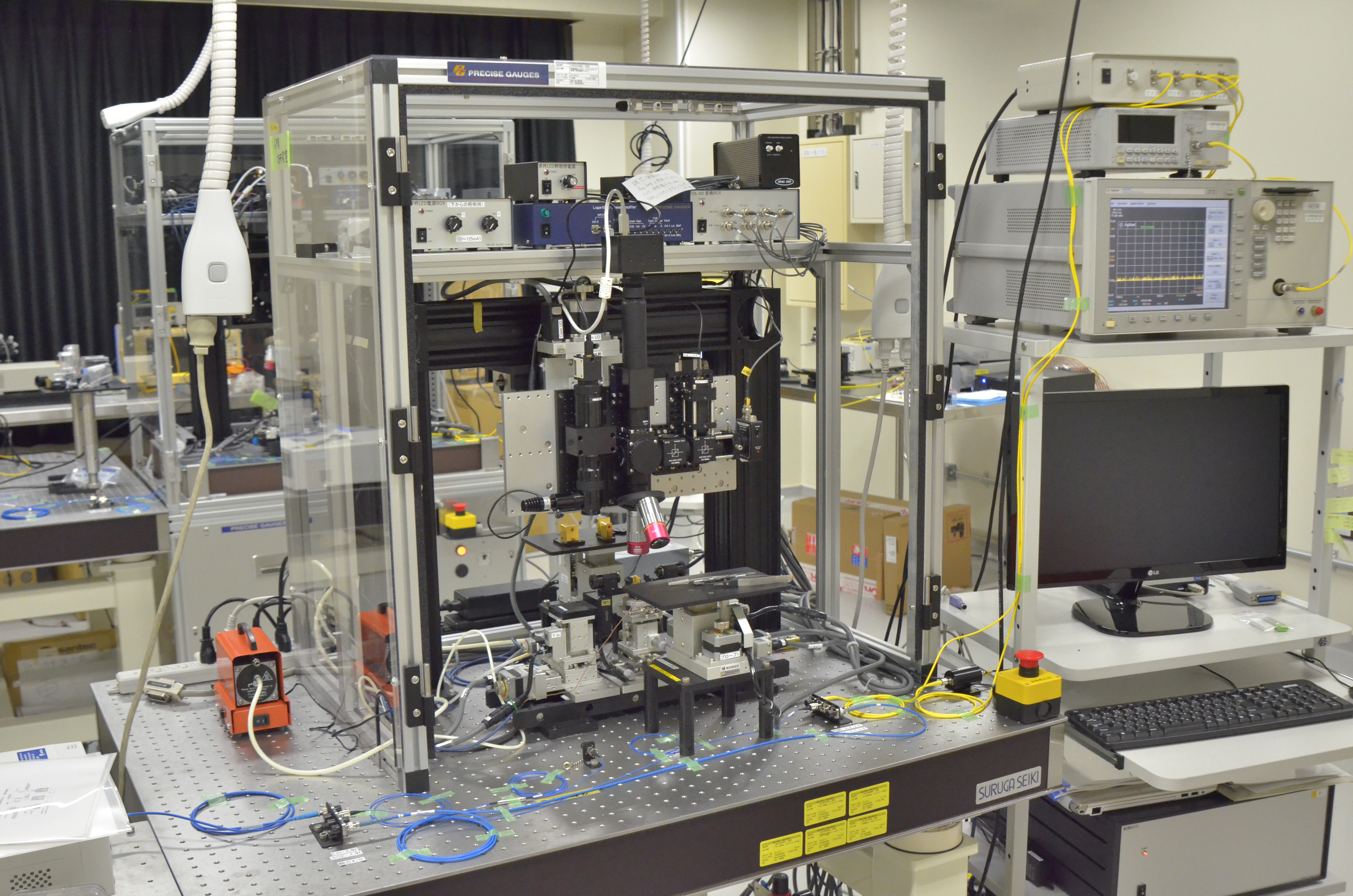
A device that can measure the transmission characteristics of multiple bar-shaped elements. Fully automatic alignment and placement of high frequency probes.
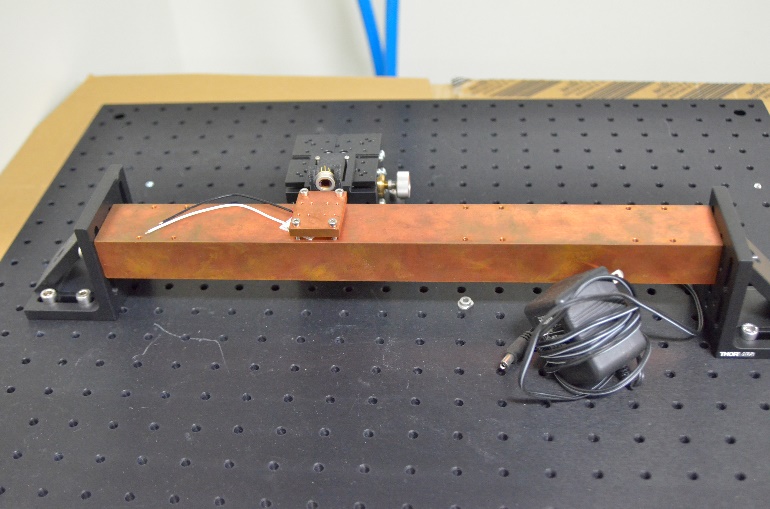
Measure waveguide loss in the green wavelength band.
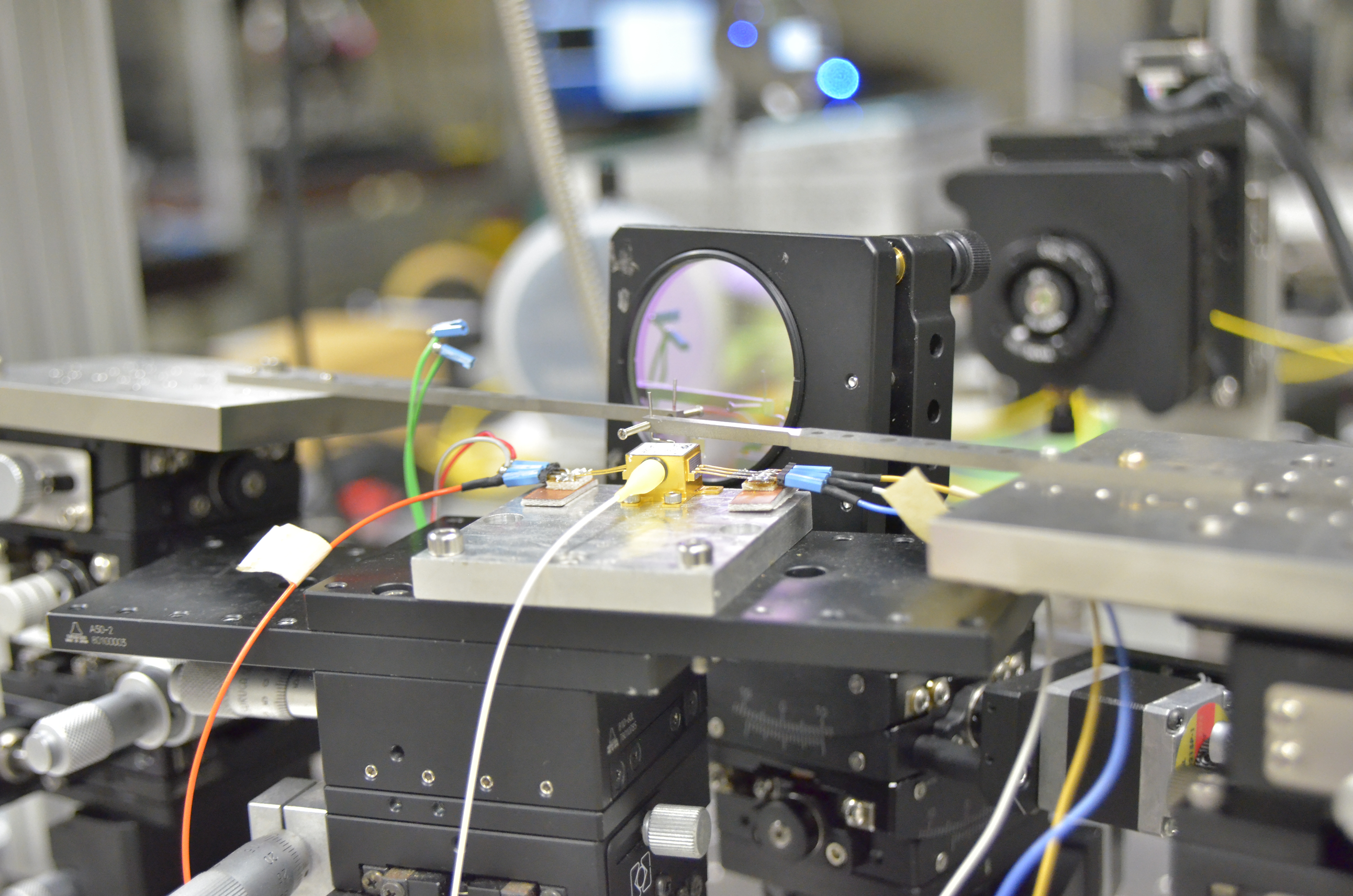
A device that can measure multiple modularized elements. Laser characteristics such as current-light and current-voltage characteristics can be measured semi-automatically.
A measurement system that inputs a high-speed signal to a semiconductor laser or an external modulator.
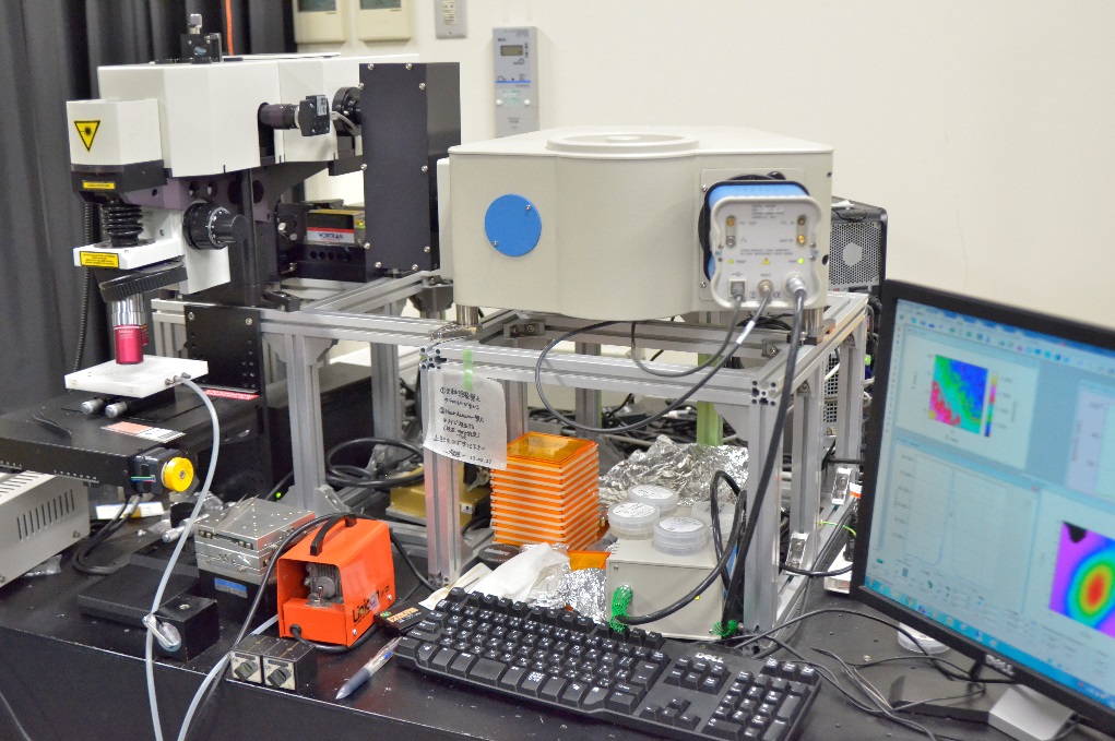
We use a pumping light source (wavelength 980nm) to excite carriers in semiconductor lasers and laminated substrates to evaluate the composition and quality of semiconductor crystals and perform laser oscillation. In addition to the micro PL of a circular beam spot, a micro PL with a spot size of 300µm x 10µm (design value) suitable for laser excitation is used.
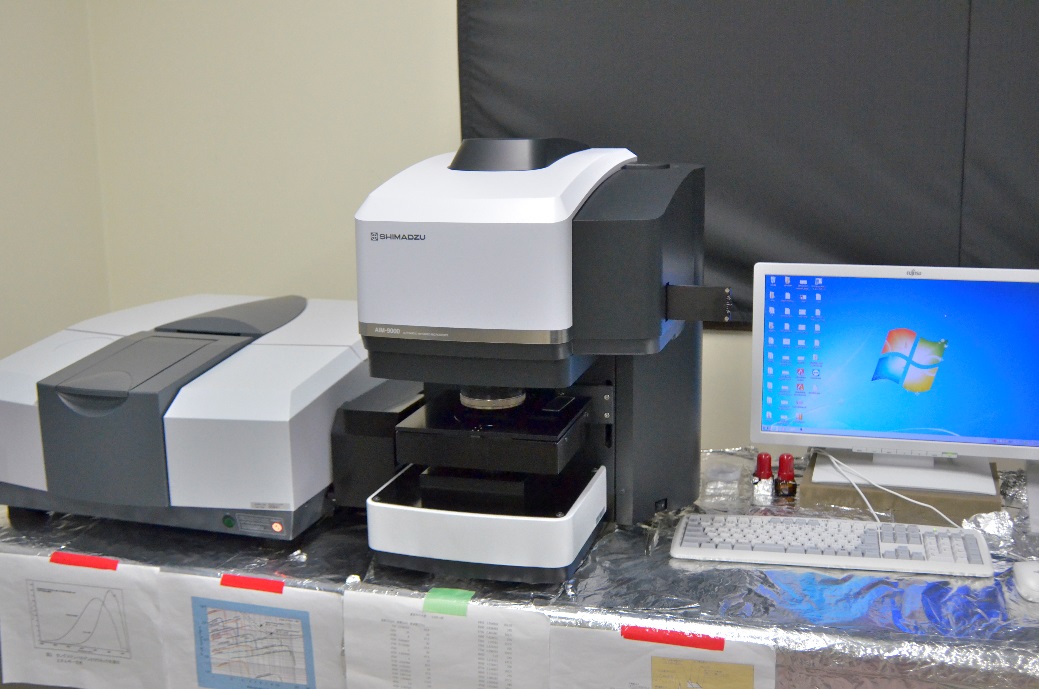
Information on the molecular structure in a minute area can be easily obtained as an infrared absorption spectrum.
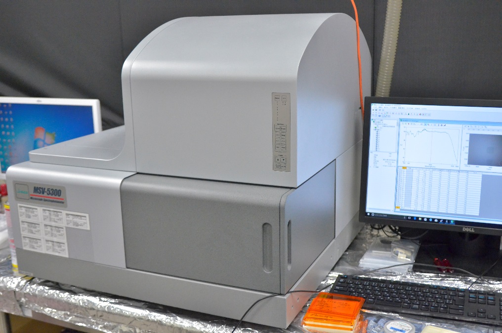
Transmission / reflection measurement of minute samples and minute parts can be performed in a wide wavelength range from ultraviolet to near infrared.
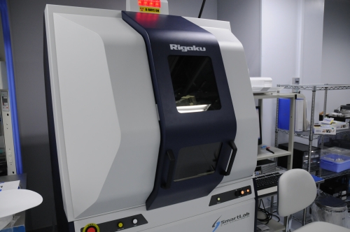
This device analyzes the layer structure of a semiconductor wafer on which a film has been formed. Measure the X-ray reflection spectrum and estimate the state of the deposited layer.
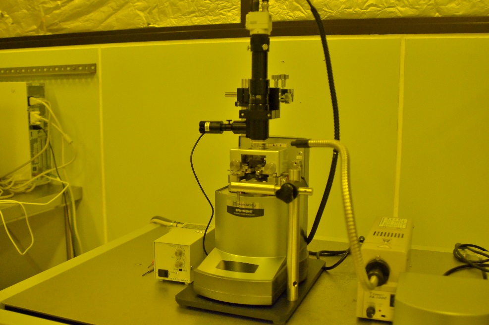
An atomic force microscope (AFM) is a type of microscope that detects the atomic force acting on a probe and a sample.
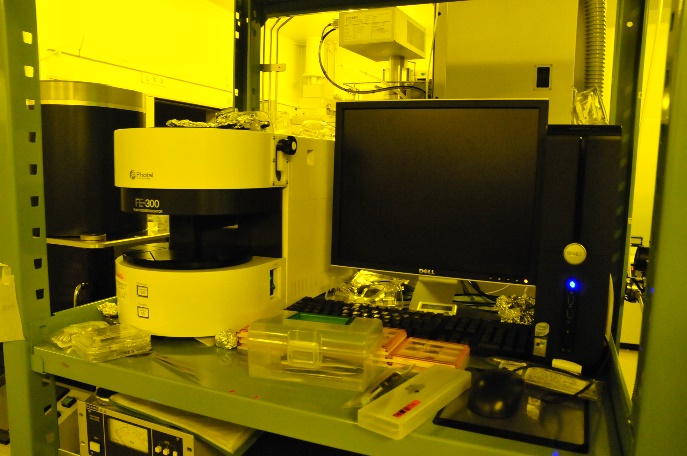
This is a device to measure the thickness of a thin film.
Accurate film thickness can be obtained by incorporating the wavelength characteristics of the refractive index and absorption coefficient of the layer to be measured.
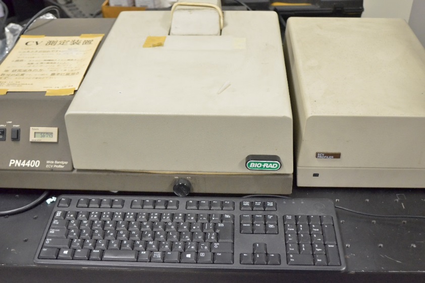
This device measures the doping concentration of semiconductors.
Measurements are made using the principle of depletion when voltage is applied.
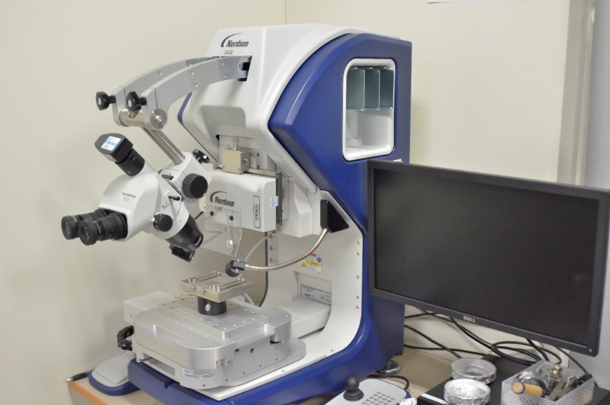
Bond tester with the highest speed and accuracy. Optimized for fast, accurate and reliable bonding tests in high volume production environments.
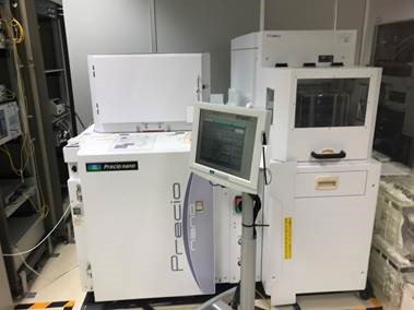
Automatic control of transmittance evaluation of optical devices on 300mm and 200mm wafers can be performed at high speed.
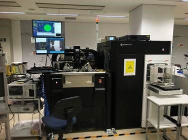
Characterization of optical devices on various substrates ranging from 300 mm wafers to small chips can be performed with automatic alignment control.
(1)PICS3D and APSYS produced by Crosslight Software Inc.
(2) Photonic Component Design Suite produced by Synopsys, Inc.
(3) FDTD Solutions, INTERCONNECT, Lumericl DEVICE and MODE Solutions produced by Lumerical Inc.
7F, S9-1, 2-12-1 O-okayama, Meguro-ku Tokyo 152-8552, Japan +81-3-5734-2555 ee.e titechnishiyama
Nishiyama lab. Student's room : South Bldg. 9 #701, #706, #707 |
Measurement room : South Bldg. 9 #604, #502, #201 |
Clean room : South Bldg. 9 #202, B1F Exposure house |
Research Laboratory of Ultra-High Speed Electronics