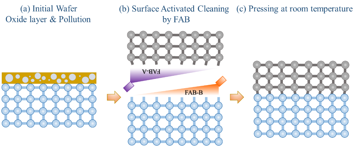
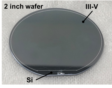
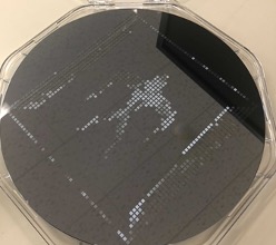
In order to realize photonic integrated circuits (PICs) consisting of active devices such as lasers and amplifiers, the hybrid integration of Ⅲ-Ⅴ compound semiconductor on silicon-on-insulator (SOI) is considered as one of solutions. Hydrophilic bonding or plasma activated bonding (PAB) are usually used for such hybrid wafer bonding. However, annealing temperature of higher than 150°C and long cooling time are required for achieving high bonding strength, resulting in the thermal stress caused by the difference between thermal expansion coefficients of bonded wafers. To deal with the mentioned problems, surface activated bonding (SAB) based on fast atom beam (FAB) was proposed in recent years, which can realize wafer bonding at room temperature. Thermal expansion between Ⅲ-Ⅴ compound semiconductor and Si could be optimized thanks to this technology, which contribute to fabricate high quality hybrid laser.
7F, S9-1, 2-12-1 O-okayama, Meguro-ku Tokyo 152-8552, Japan +81-3-5734-2555 ee.e titechnishiyama
Nishiyama lab. Student's room : South Bldg. 9 #701, #706, #707 |
Measurement room : South Bldg. 9 #604, #502, #201 |
Clean room : South Bldg. 9 #202, B1F Exposure house |
Research Laboratory of Ultra-High Speed Electronics