Optical circuits and optical networks are being installed everywhere from long-haul to inter/intra chip networks due to the high capacity of their data rate. On the other hand, because of the wider bandwidth capability compared to microwaves used in conventional wireless communication systems, sub-THz and THz waves are expected to be crucial frequency-bands in next generation wireless communication systems. Therefore, it is very important to realize a direct signal conversion method between THz wave signals and optical signals. We propose a novel structure of optical to THz signal converter consisting of a plasmon waveguide at THz range.
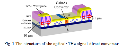
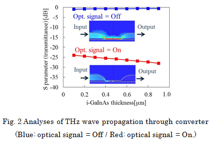
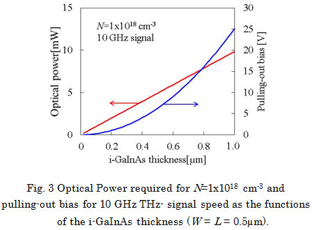
Figure 1 shows the conceptual diagram of the optical-THz signal converter on semi-insulating InP substrate. The THz wave propagates through the microstrip waveguide consisting of n+-GaInAs (~1×1019 cm-3)/i-GaInAsP/benzocyclobutene (BCB)/Ti/Au layer. The n+-GaInAs layer acts as a bottom metal ground since the imaginary part of the refractive index is enough large for THz signal. At the middle of this THz waveguide, the THz wave propagates into a converter section consisting of n+-GaInAs (~1×1019 cm-3)/i-GaInAs/p+-GaInAs (~1×1019 cm-3)/Ti/Au layer. The size of this converter is much smaller than the spot size of THz wave and the propagation through such a small converter can be achieved by utilizing plasmonic effect. When 1.55 µm optical signals are input into the GaInAs layer from an integrated optical waveguide at the side of the converter section, free carriers are generated due to the photon absorption as the bandgap energy of the GaInAs is smaller than the photon energy. In this case, the converter section acts as metallic wall by free carrier absorption and skin effect, resulting in decreasing the transmittance of THz waves. On the other hand, THz waves can transmit when the optical signals are switched off. Therefore, the THz waves can be modulated by the optical signals injected into the GaInAs converter section.
Figure 2 shows the analyzed transmission of THz wave. In this calculation, the carrier density in the i-GaInAs was assumed to be 5×1016 cm-3 (opt. signal = Off) or 1×1018 cm-3 (opt. signal = On). Although longer i-GaInAs layer led to larger extinction ratio, over 20 dB extinction ratio can be achieved even with the length of 0.1 µm.
The modulation speed of THz signals is determined by free carrier lifetime. To enhance modulation bandwidth, pulling-out bias can be applied to p+-GaInAs/i-GaInAs/n+-GaInAs structure in the converter section.
Figure 3 shows the required optical power for a carrier density of N = 1×1018 cm-3 (the red line) and required pulling-out bias for 10 GHz THz signal (the blue line). With this structure, the optical signal power and the bias voltage can be suppressed to less than 10 mW and 10 V, if the thickness of i-GaInAs is less than 0.6 µm. For thinner i-GaInAs thickness, higher modulation speed can be possible.
7F, S9-1, 2-12-1 O-okayama, Meguro-ku Tokyo 152-8552, Japan +81-3-5734-2555 ee.e titechnishiyama
Nishiyama lab. Student's room : South Bldg. 9 #701, #706, #707 |
Measurement room : South Bldg. 9 #604, #502, #201 |
Clean room : South Bldg. 9 #202, B1F Exposure house |
Research Laboratory of Ultra-High Speed Electronics