Si LSIs have rapidly increased the degree of their integration and incorporated all components needed for computers and other applications (e.g. SoC). This has greatly raised the processing capability and reduced the total power dissipation of electronic systems. However, RC time delay in metal interconnection has become a dominant limiting factor on system performance, which is known as an ‘interconnect bottleneck.’
To overcome the bottleneck, one promising method is to use on-chip optical interconnection instead of electrical wiring. Optical interconnection is negligible from transmission delay and electromagnetic interference; besides, it is compatible with multiplexing large-capacity data transmission. Therefore, optical interconnection is superior to electrical ones if it can be easily combined with Si LSIs.
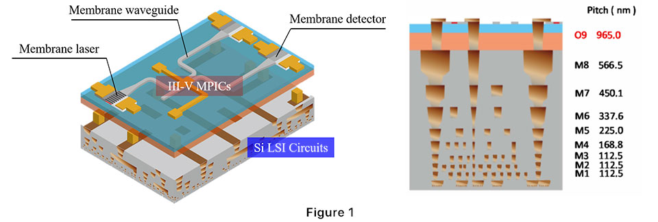
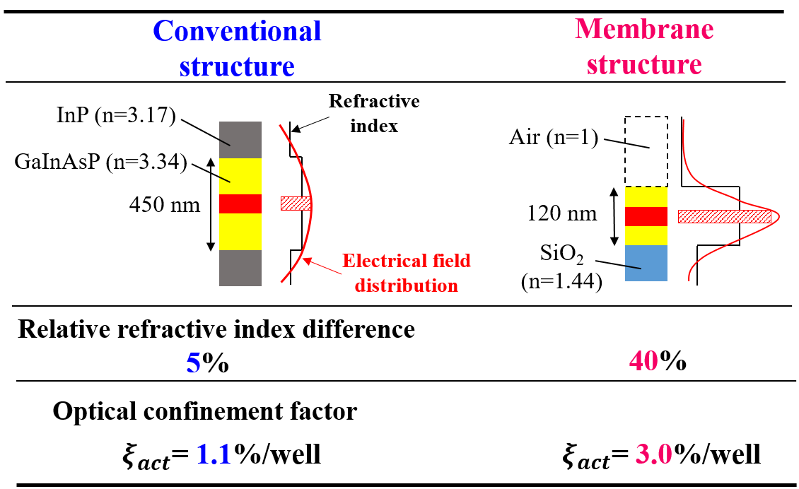
To put optical interconnection into practical use, we proposed a method of hybrid optical-electrical interconnection that uses InP-based membrane photonic integrated circuits (Fig. 1). The InP-based membrane (O9) with optical data-transmission circuits is attached on a Si LSI chip with multilevel interconnection (M1-M8) using adhesive bonding. The lasers and detectors in the data-transmission circuits are connected to driving and amplifying circuits on the Si LSI using through-silicon vias. The point of our idea is to make the GaInAsP core of waveguides in a form of a membrane (thin film) sandwiched between Si02 and air (see Fig. 2). Strong optical confinement in the core can be obtained because of the large relative refractive index difference. This enhanced optical confinement of the core layer greatly improves the performance of a series of optical devices.
7F, S9-1, 2-12-1 O-okayama, Meguro-ku Tokyo 152-8552, Japan +81-3-5734-2555 ee.e titechnishiyama
Nishiyama lab. Student's room : South Bldg. 9 #701, #706, #707 |
Measurement room : South Bldg. 9 #604, #502, #201 |
Clean room : South Bldg. 9 #202, B1F Exposure house |
Research Laboratory of Ultra-High Speed Electronics