Research : Optical Integrated Circuits on LSIs
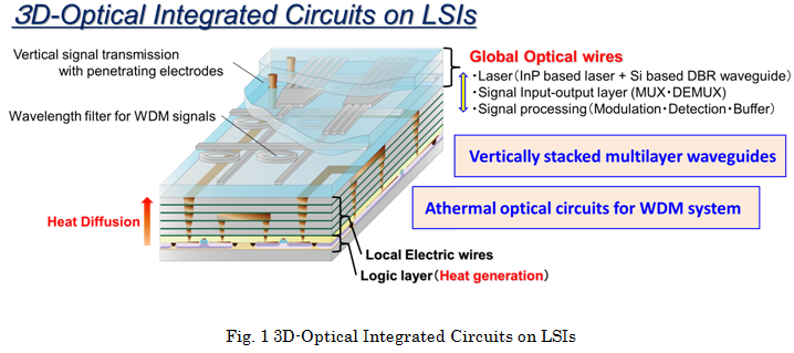
Appearances of a high-capacity and high quality media, such as 3D-movies and videos have led higher data transaction capability of LSIs. The required clock frequency and total data stream for LSI chips are expected to exceed 5 GHz and several Tera-bits/sec by 2019. For achieving the requirement, miniaturization technology of the complementary metal oxide semiconductor (CMOS) transistors can enhance the operation speed of the local wire layer. On the other hand, the signal delay in the global metallic wires, which connect between blocks in a LSI-chip, is limiting the total LSI performance due to the skin effect. As one of the long-term solutions, introduction of optical circuits on the LSIs is proposed as well as 3D-LSI chip technology. And for the optical circuits on the LSIs, silicon photonics technology have evolved drastically during the past ten years due to the superiority in the integration of electronics and photonics, which are both based on the same silicon-platform. Our research group has mainly challenged to the following two topics.
Ⅰ. Athermal wavelength filters toward optical interconnection to LSIs
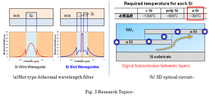
Our research group targets the monolithic integration of optical circuit with electronic LSI circuits. Then, one of the problems to be solved is the wavelength shift to long wavelength side caused by the thermal diffusion from the logic layer in Si-LSI because of the large positive temperature coefficient of refractive index of Si. This effect is wrong to the wavelength filter for Wavelength Division Multiplexing (WDM) systems. For the solution, I proposed an athermal Si slot waveguides embedded with benzocyclobutene (BCB), which is the low-k polymer material for electronics. The slot waveguide can confine the light in the central low index area (Fig.1). By controlling the widths of the waveguide and slot-gap, the temperature coefficient of equivalent index could be zero.
The fabricated athermal ring resonator and MZI have the temperature dependence of the drop wavelengths was as small as -0.6 and 0.9 pm/K, respectively, which are small enough to use as wavelength filters with compare to a conventional long haul 100GHz-WDM system. As a next stage, wavelength trimming technology with deep ultra-violet (DUV) irradiation has been investigated.
Ⅱ. Amorphous-silicon multilayer waveguides vertically stacked on SOI substrate
Silicon is the main material for the optical circuit. To integrate the optical components on a LSI chip, all the fabrication processes for the optical components should be regulated to below 400°C in order to avoid damages to the electrical circuits. Amorphous silicon is the most promising material for optical circuits since it can be deposited under low-temperature conditions. Moreover, by stacking amorphous silicon and cladding material alternatively, high-density 3-dimensional optical circuits can thereby be realized on the LSI. Fig 3(b) illustrates the vertical signal transmission using grating coupler between two layers. Using metal reflector under the grating coupler, more than 80% of layer-to-layer coupling efficiency was obtained with 3D Finite Difference Time Domain (FDTD) method.
List of reports
Journal Papers
- (1) K. Inoue, D. Plumwongrot, N. Nishiyama, S. Sakamoto, H. Enomoto, S. Tamura, T. Maruyama, and S. Arai, “Loss Reduction of Si Wire Waveguide Fabricated by Edge-Enhancement Writing for Electron Beam Lithography and Reactive Ion Etching Using Double Layered Resist Mask with C60,” Jpn. J. Appl. Phys., vol. 48, no. 3, pp. 030208-1-3, Mar. 2009.
- (2) Y. Atsumi, K. Inoue, N. Nishiyama, and S. Arai, “Athermal Wavelength Characteristics of Si Slot Ring Resonator Embedded with Benzocyclobutene for Optoelectronic Integrated Circuits,” Jpn. J. Appl . Phys., vol. 49, pp. 050206-1-3, May. 2010.
- (3) J. Kang, Y. Atsumi, M. Oda, T. Amemiya, N. Nishiyama, S. Arai, “Low-loss Amorphous Silicon Multilayer Waveguides Vertically Stacked on Silicon-on-Insulator Substrate,” Jpn. J. Appl. Phys., Vol. 50, No. 12, pp. 120208-1-3, Nov. 2011.
- (4) Y. Atsumi, M. Oda, J. Kang, N. Nishiyama, and S. Arai, “Athermal Wavelength Filters toward Optical Interconnection to LSIs,” IEICE Trans. Electron., vol. E95-C, no. 2, pp. 229-236, Feb. 2012.
International Conferences
- (1) Y. Atsumi, N. Nishiyama, H. Enomoto, K. Inoue, and S. Arai, “Athermal Wavelength Property of Si-Slot Ring Resonator Embedded with Benzocyclobutene.” The 6th IEEE International Conference on Group IV Photonics (GFP). San Francisco (California), ThB3, Sep. 2009
- (2) J. Kang, K. Inoue, Y. Atsumi, N. Nishiyama, and S. Arai, “Loss Measurement of Multiple Layer a-Si Waveguides toward 3D Si-Optical Circuits,” 2010 Int. Conf. on Solid State Devices and Materials (SSDM 2010), Tokyo (Japan), D-8-2, Sep. 2010.
- (3) Y. Atsumi, J. Kang, Y. Maeda, M. Oda, N. Nishiyama, and S. Arai, “Low-Loss Si-Slot Waveguides and Ring Resonator Embedded with Benzocyclobutene,” The 23rd Annual Meeting of the IEEE Photonics Society (PHO 2010), Denver, Colorado (USA), TuP-3, Nov. 2010
- (4) Y. Atsumi, M. Oda, J. Kang, N. Nishiyama, and S. Arai, “Wide-gap Athermal Si-Slot Mach-Zhender Interferometer Embedded with Benzocyclobutene.” The 8th IEEE International Conference on Group IV Photonics (GFP). London (U.K.), FC7, Sep. 2011
- (5) J. Kang, Y. Nishikawa, Y. Atsumi, M. Oda, T. Amemiya, N. Nishiyama, and S. Arai, “Amorphous Silicon Grating-Type Layer-to-Layer Couplers for Intra-Chip Connection,” 2012 IEEE Optical Interconnects Conference (OIC-2012), TuD3, May. 2012.
Domestic Conferences
- (1) K. Inoue, D. Plumwongrot, N. Nishiyama, S. Sakamoto, H. Enomoto, S. Tamura, T. Maruyama, S. Arai:「C60含有と非含有EBレジストZEPの重ね塗りによるSi導波路ドライエッチング形状の向上」. The 55th Spring Meeting, 2008, The Japan Society of Applied Physics and Related Societies, 29p-ZG-15, Chiba, Mar. 2008.
Tokyo, Mar. 2001.
- (2) Y. Atsumi, N. Nishiyama, H. Enomoto, K. Inoue, and S. Arai:「BCB埋め込みSiスロット導波路による波長フィルタの温度無依存化の検討」, The 56th Spring Meeting, 2009, The Japan Society of Applied Physics and Related Societies, 1a-B-12, Digest III, Ibaraki, Japan, Mar/Apr. 2009.
- (3) Y. Atsumi,K. Inoue,N. Nishiyama,and S. Arai: 「BCB埋め込みSiスロット導波路構造を用いた温度無依存波長フィルタ」The 2009 IEICE Society Conf., C-3-7, Niigata, Japan, Sept. 2009.
- (4) K. Inoue,Y. Atsumi,N. Nishiyama,S. Tamura,and S. Arai:「SOI基板上多層a-Si細線導波路の伝搬特性の評価」The 57th Spring Meeting, The Japan Society of Applied Physics and Related Societies, 17p-P3-7, Kanagawa, Japan, Mar. 2010.
- (5) Y. Atsumi,K. Inoue,N. Nishiyama,and S. Arai:「BCB埋め込みSiスロット導波路の光伝搬損失の評価」The 57th Spring Meeting, The Japan Society of Applied Physics and Related Societies, 17p-P3-10, Kanagawa, Japan, Mar. 2010.
- (6) Y. Atsumi, J. Kang, Y. Maeda, M. Oda, N. Nishiyama, and S.Arai:「BCB埋め込みスロットリング共振器の低損失化」 The 71st Autumn Meeting, The Japan Society of Applied Physics, 14p-G-16, Nagasaki, Japan, Sep. 2010.
- (7) Y. Atsumi, M. Oda, J. Kang, N. Nishiyama, and S.Arai:「幅広ギャップ構造を有するBCB 埋め込み温度無依存SiスロットMZI」The 58th Spring Meeting, The Japan Society of Applied Physics and Related Societies, 24a-KB-8, Kanagawa, Japan, Mar. 2011.
- (8) J. Kang, Y. Atsumi, N. Nishiyama, and S.Arai:「多層化されたアモルファスシリコン細線導波路の低損失伝搬特性」 The 58th Spring Meeting, The Japan Society of Applied Physics and Related Societies, 24a-KB-9, Kanagawa, Japan, Mar. 2011.
- (9) Y. Atsumi, M. Oda, J. Kang, N. Nishiyama, and S.Arai:「幅広ギャップ構造を有する温度無依存BCB埋め込みSiスロット型リング共振器」The 72nd Autumn Meeting, The Japan Society of Applied Physics and Related Societies, 2a-ZN-9, Yamagata, Japan, Sept. 2011
- (10) M. Oda, Y. Atsumi, J. Kang, T. Koguchi, T. Amemiya, N. Nishiyama, and S. Arai:「BCB 埋め込み温度無依存Si スロットMZI 型波長フィルタ信号伝送特性の温度依存性」, The 2011 IEICE Society Conf., C-3-49, Hokkaido, Japan, Sept. 2011
- (11) J. Kang, Y. Nishikawa, Y. Atsumi, M. Oda, T. Amemiya, N. Nishiyama, and S. Arai:「多層アモルファスシリコン細線導波路間の信号伝送用グレーティングカプラ」, The 2012 IEICE General Conf., C-3-38, Tokyo, Japan, Mar. 2012..
- (12) M. Oda, Y. Atsumi, T. Sifer, J. Kang, T. Amemiya, N. Nishiyama, S. Arai:「温度無依存BCB 埋め込みSi スロットリング共振器を用いたドロップフィルタ」, The 2012 IEICE General Conf., C-3-39, Tokyo, Japan, Mar. 2012
- (13) Y. Atsumi, J. Kang, Y. Nishikawa, M. Oda, T. Amemiya, N.Nishiyama, and S. Arai:「ブロッホ波干渉型低損失連結クロス導波路の作製評価」The 59th Spring Meeting, The Japan Society of Applied Physics and Related Societies, 18a-GP4-22, Tokyo, Japan, Mar. 2011.
- (14) J. Kang, Y. Atsumi, T. Sifer, T. Amemiya, N. Nishiyama, and S. Arai:「金属ミラー付き多層アモルファスシリコン細線導波路間のグレーティングカプラ」The 2012 IEICE Society Conf., C-3-59, Toyama, Japan, Sept. 2011.
- (15) T. Sifer, Y. Atsumi, J. Kang, N. Nishiyama, and S. Arai, 「紫外線照射を用いた温度無依存シリコンスロットリング共振器の波長トリミング」The 73rd Autumn Meeting, The Japan Society of Applied Physics and Related Societies, 12p-C5-17, Ehime, Japan, Sept. 2011.
Nishiyama Laboratory
School of Engineering Dept. of Electrical and Electronic Engineering, Institute of Science Tokyo
7F, S9-1, 2-12-1 O-okayama, Meguro-ku Tokyo 152-8552, Japan
+81-3-5734-2555
ee.e titechnishiyama
Nishiyama lab. Student's room : South Bldg. 9 #701, #706, #707 |
Measurement room : South Bldg. 9 #604, #502, #201 |
Clean room : South Bldg. 9 #202, B1F Exposure house |
Research Laboratory of Ultra-High Speed Electronics