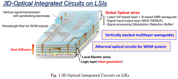
Appearances of a high-capacity and high quality media, such as 3D-movies and videos have led higher data transaction capability of LSIs. The required clock frequency and total data stream for LSI chips are expected to exceed 5 GHz and several Tera-bits/sec by 2019. For achieving the requirement, miniaturization technology of the complementary metal oxide semiconductor (CMOS) transistors can enhance the operation speed of the local wire layer. On the other hand, the signal delay in the global metallic wires, which connect between blocks in a LSI-chip, is limiting the total LSI performance due to the skin effect. As one of the long-term solutions, introduction of optical circuits on the LSIs is proposed as well as 3D-LSI chip technology. And for the optical circuits on the LSIs, silicon photonics technology have evolved drastically during the past ten years due to the superiority in the integration of electronics and photonics, which are both based on the same silicon-platform. Our research group has mainly challenged to the following two topics.
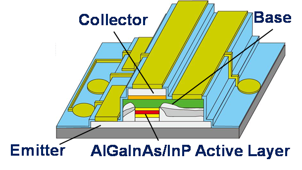
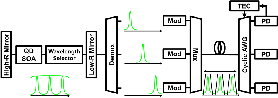
We propose a new light source “Transistor Laser (TL)” for next generation optical communication. Different from Laser Diodes (LDs), TL has 3 terminals; emitter, base, and collector. Electrons injected from an emitter are diffused, and a portion of the electrons is recombined at the active layer while the rest are removed from the collector. Due to this carrier flow, fast carrier supply to the active layer is realized and as a result, high-speed modulation beyond conventional LDs can be achieved. Now, we start demonstrating modulation with TL.
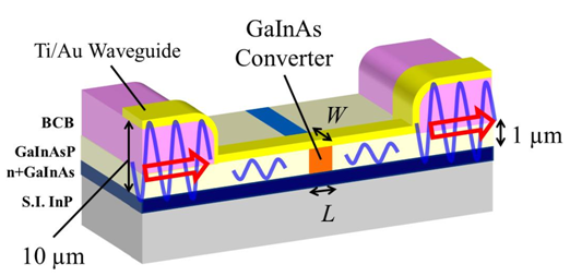
Optical circuits and optical networks are being installed everywhere from long-haul to inter/intra chip networks due to the high capacity of their data rate. On the other hand, because of the wider bandwidth capability compared to microwaves used in conventional wireless communication systems, sub-THz and THz waves are expected to be crucial frequency-bands in next generation wireless communication systems. Therefore, it is very important to realize a direct signal conversion method between THz wave signals and optical signals. Until now, we devised a novel direct converter structure utilizing photo carrier generated gate in THz waveguide and analyzed its fundamental characteristics.
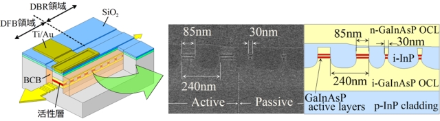
We propose a new method of monolithic integration by using the energy blue shift due to the lateral quantum confinement effect. Using this technique, we realize a new type of distributed reflector (DR) laser consisting of a DFB section with wirelike active regions and a distributed Bragg reflector (DBR) section with a quantum-wire structure.
For low threshold and high efficiency operation, we designed the low-loss waveguide using the energy blue shift due to the lateral quantum confinement effect. As a result, the DR laser with the low-threshold, high efficiency and single-mode operation can be achieved.
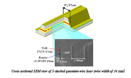
We realized a RT-CW operation of GaInAsP/InP quantum-wire lasers (wire width of 23 nm in a period of 80 nm, 5-stacked quantum-wires) fabricated by EB lithography, CH4/H2-reactive ion etching and 2-step OMVPE growth processes for the first time. From RT-CW lifetime measurement, no noticeable performance degradation was observed even after more than 12,000 hours. Good size distributions of multiple-quantum-wire structures have been obtained with standard deviations less than ±2 nm.
GaInAsP/InP quantum-wire lasers with narrow wire structures (wire width of 14 nm in a period of 80 nm, 5-stacked quantum-wires) were realized. Lateral quantum confinement effect in this quantum-wire laser could be observed via sharper shape of the EL spectrum than that of quantum-film lasers in the higher transition energy region.
In future, we aim to realize the narrow spectral width with good size uniformity of quantum-wires and the low threshold current operation of Q-Wire lasers by applications of distributed Bragg reflector (DBR) structure and DFB cavity.
Although DFB lasers with partially etched quantum wells have been reported from several reseach groups, excellent characteristics of DFB lasers with completely etched wirelike active regions are experimentally shown. Threshold current dependence on the laser with wirelike active regions is investigated. And also, superior lasing properties of this type of BH-DFB LD, such as submilliampere and stable single-mode operations will be given.

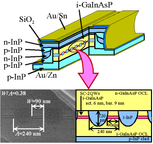
Optical metamaterials offer new opportunities for innovation in the field of electromagnetic parameter design, such as the design of permittivity ε and permeability µ. The major focus of attention is to create artificial materials with unique ε-µ values that cannot be observed in any existing media and to take advantage of these expanded parameters for better control of electromagnetic waves. Recent progress in optical metamaterials has allowed researchers to move material properties away from the non-magnetic line µ = 1 and has opened the third quadrant of the parameter space (i.e., ε<0 and simultaneously µ<0), which was previously inaccessible. One of the next trends is to think of metamaterials as devices, where the structuring of metal and the hybridization with functional agents brings new functionality. Especially, introducing optical metamaterials into actual photonic devices poses an exciting challenge. Much effort has been expended in the development of advanced optical applications using the concept of metamaterials. In our laboratory, we demonstrate InP-based optical devices combined with metamaterials to show the possibility of permeability control on the semiconductor-based photonics platform.
Under Construction
7F, S9-1, 2-12-1 O-okayama, Meguro-ku Tokyo 152-8552, Japan +81-3-5734-2555 ee.e titechnishiyama
Nishiyama lab. Student's room : South Bldg. 9 #701, #706, #707 |
Measurement room : South Bldg. 9 #604, #502, #201 |
Clean room : South Bldg. 9 #202, B1F Exposure house |
Research Laboratory of Ultra-High Speed Electronics